Continue to Site

Welcome to our site!

Electro Tech is an online community (with over 170,000 members) who enjoy talking about and building electronic circuits, projects and gadgets. To participate you need to register. Registration is free. Click here to register now.

  • Welcome to our site! Electro Tech is an online community (with over 170,000 members) who enjoy talking about and building electronic circuits, projects and gadgets. To participate you need to register. Registration is free. Click here to register now.

555 timer flyback driver circuit problem

Status
Not open for further replies.

Fluffyboii

Active Member
Hi,
I was trying to make an op amp circuit work from 5V USB power and lack of dual power supply was making it very difficult as always. One way of solving the problem would be using 7660 IC as Nigel suggested. And it seems like a brilliant solution. But I already made an order for electronic parts form an online warehouse and I don't want to make a new order to buy a single IC and pay shipping costs.
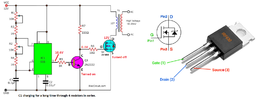
So I was thinking of making some kind of isolated boost converter with the stuff I have at hand. There are multiple ways of getting some kind of AC waveform and feeding it to a transformer to increase its voltage then rectify it. I have decided to use a 555 timer to generate high frequency pulses. Then I could split the AC I get from transformer to get positive and negative voltages as I wanted. I also had a small flyback transformer left from an kit I failed to build some time ago so at worst case scenario it would be used with that. First circuit that comes when Googled is the one at the bottom.
1672758328914.png

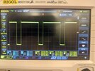
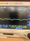
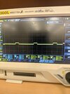
I made it and test it. The frequency was about 1Khz which was too low for driving a flyback but I gave it a go anyway. It consumes about 2A at 3V when flyback transformer is connected because I limited the current so it is not sustainable at 12V. I checked the waveforms at the BJT and it seems like circuit sends some chonky high duty rate pulses to the BJT and it gets inverted to small duty cycle pulses for the Mosfet to do the switching. My choice of mosfet here is IRF630 which I believe should function similarly. The problem is the waveform 555 generates and what shows up at the base of the BJT is quite different. For some reason there is a huge voltage drop at the base of the BJT. In turn it shows up as a very small voltage at collector and at the Mosfet's gate. And I believe because of that reason Mosfet doesn't really do any switching and instead stays open all the time causing huge current to flow. I am putting oscilloscope photos to bottom so you can see how small the voltage gets at the base and collector.
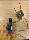
I believed that the 1K resistor was too high and switched it with 100 ohms instead. I also decreased the timing capacitor with 10nF increasing the switching to about 100Khz. This did not change anything. I basically switched to this circuit:
1672759008932.png

Sooo what I am exactly doing wrong here. I believe 555 part is functioning, BJT is connected right and I did not mixed up the Mosfet connections as well this time. Should I put some series resistance with the gate do decrease current. I actually got some high voltage randomly at the output when I tested it but that was one time only and my 555 blow up later. Now I am sure everything is connected right. If I can get this to work I will use a transformer with small turn ratio and use a bridge rectifier to get my positive and negative rails. If the output signal is full of garbage ripples I will use linear converters to cut it off. Are there any similar oscillator circuits to get a quick dirty AC wave. I doubt lack of feedback will be an issue since my load will be few op amps pulling less than 10mA at total.

The more I think about it stupider it feels that I went with this instead of doing anything else.
 

Attachments

  • IMG_20230103_174427.jpg
    IMG_20230103_174427.jpg
    528.4 KB · Views: 215
  • IMG_20230103_174534.jpg
    IMG_20230103_174534.jpg
    489.7 KB · Views: 175
  • IMG_20230103_174555.jpg
    IMG_20230103_174555.jpg
    518.9 KB · Views: 214
  • IMG_20230103_181749.jpg
    IMG_20230103_181749.jpg
    725.7 KB · Views: 302
Last edited:
The frequency was about 1Khz
If I'm reading your first scope picture (.....749) correctly it seems to be showing a pulse frequency of 12.9kHz ?
It's not clear where your scope probes were connected. Is that >90V shown in the first pic?
 
If I'm reading your first scope picture (.....749) correctly it seems to be showing a pulse frequency of 12.9kHz ?
It's not clear where your scope probes were connected. Is that >90V shown in the first pic?
Yes frequency is around 10K, I messed with the pots a little. I am sure voltage is not 90V at the 3th pin of the 555. Probe setting or something must be wrong.
 
Disconnect the base of the transistor and measure the gate voltage on the mosfet?
Also double-check the mosfet connections?
Sure. I must add that I took the measurements with no coil attached. It doesn't go into meltdown without the load. Checking mosfet again I see that is is connected correctly and I did not get fooled by the gate being at the 1st pin. 2n2222 also seems to be correct. It looks like it is supposed to pull 3A at 12V so it is pulling considerably more. I will try removing base connection tomorrow. Anything else I can try? Wouldn't mosfet gate have full line voltage if there was no connection of the base of the BJT.
 
Your circuit seems a bit OTT if all you want is a negative supply for an op-amp. Wouldn't something such as this suffice? :-
1672766096089.png

Edit: Oops. C3 should be t'other way up!
 
Last edited:
Your circuit seems a bit OTT if all you want is a negative supply for an op-amp. Wouldn't something such as this suffice? :-
View attachment 139816
It certainly would be. Seems much simpler as well than what I was trying to do. I will try it. But I will try to fix the thing I tried to build as well so I can use it with the small flyback. Should I use silicon diodes or something with less Vd.
 
Last edited:
Fluffy, your 555 has its timing capacitor charging for a long time by two resistors in series producing an output high that turns on the transistors and transformer. Then the 555 timing capacitor is discharged by only one resistor for a short time when the 555 output is low and the transistors and transformer are turned off.
It would be the opposite if the transistor inverter is removed so that the output of the 555 drives the gate of the Mosfet.
Yes. My problem is that voltages at the transistor base and mosfet gate are very small and it is causing a huge current to be drawn from the drain of the mosfet.
 
Right now it is just like a electromagnet. When I give it sudden voltage from battery I can feel the movement of flyback transformer. No high voltage is generated because Mosfet is not switching because its gate voltage never goes zero. I think I will just replace the BJT and see what happens.
 
The collector of the transistor should go up to the 12V supply and go down almost to 0V.
When the collector of the transistor goes to 12V then the Mosfet turns on and its drain goes to 0V.
When the collector of the transistor goes to near 0V then the Mosfet turns off and its drain goes to 12V.
Your Mosfet is always turned on so it must be connected wrong or it is defective.
 

Attachments

  • IRF630.png
    IRF630.png
    374.5 KB · Views: 287
The collector of the transistor should go up to the 12V supply and go down almost to 0V.
When the collector of the transistor goes to 12V then the Mosfet turns on and its drain goes to 0V.
When the collector of the transistor goes to near 0V then the Mosfet turns off and its drain goes to 12V.
Your Mosfet is always turned on so it must be connected wrong or it is defective.
I am aware how it works. The problem is that when I checked it with the oscilloscope, I saw that there were high voltage pulses getting out of the 555 output pin but at the base of the transistor these waves were attenuated greatly. At the collector of the NPN transistor there was some positive DC voltage about 8 volts that never actually went to zero and on top of that there was a very small inverted pulse signal. Because collector voltage never goes to zero Mosfet always stays open. When I first put it together it actually worked for a while then happened to be like this. I think NPN transistor is damaged, or the Mosfet. But I always had current limiting on my power supply so Mosfet never got a current passing from its drain to source that passes its maximum value which is 9A. So unless I somehow generated a very high voltage spike at its base there should be no reason for it to be damaged. I used the pin diagram you put in the photo for the Mosfet. Actually this bothers me a lot so lemme change the NPN transistor and see if that solves it.


Ok Mosfet become a resistor apparently. It always has to be the mosfet that shits the bed since it is the most expensive. I hate it.

I changed it with an IRF1740 I salvaged from a CRT long ago. CRT loot is always the best since I get multiple free heatsinks and high voltage components.

Do I need those two pots though. The fact that I can change the frequency and the sound is cool and all but its performance doesn't really change. I wonder if going with a higher frequency would help.
 
Last edited:
It is odd that it goes over 10Khz when it should not go more than 5Khz according to calculator. Maybe my capacitor is lower than it is branded. Still seems like too much margin error. Should I try 1nF and see if going to 40Khz makes it more efficient. I think it should operate out of human hearing range for that flyback to work nicely. Ignore this. With both 10K pots it should be able to go up to 100Khz. Since I removed one it can only go up to 11Khz. Seems like sweet spot is around lower frequencies anyway. Coil and Mosfet heats up too fast to figure where exactly it is.
1672788842363.png


1672788992957.png
 

Attachments

  • 1672788739383.png
    1672788739383.png
    195.5 KB · Views: 164
Last edited:
The base-emitter of a transistor is a 0.7V diode. Then the base voltage is 0.7 when it is turned on and is 0V when it is turned off.
The 11.9V in the 330 ohms collector resistor causes 36mA and the base current should be 1/10th at 3.6mA.
With a 1k base resistor then the base current was (10.6V- 0.7V)/1k= 9.9mA which is high but should work fine.
The base resistor should be increased to 2.7k.

But instead you reduced the base resistor to 100 ohms which probably destroyed the transistor.

The high voltage transformer probably fed a spark over to the transistor and Mosfet.
 
The voltage at the base of an NPN bjt whos emitter is grounded will never get above ~0.6 Volts. This is because the Base-Emitter junction is effectively a diode.
 
The datasheet of an LM555 shows a graph at about 4.7kHz and its calculation of 4.8kHz when the two timing resistors are each 10k.
 
The base-emitter of a transistor is a 0.7V diode. Then the base voltage is 0.7 when it is turned on and is 0V when it is turned off.
The 11.9V in the 330 ohms collector resistor causes 36mA and the base current should be 1/10th at 3.6mA.
With a 1k base resistor then the base current was (10.6V- 0.7V)/1k= 9.9mA which is high but should work fine.
The base resistor should be increased to 2.7k.

But instead you reduced the base resistor to 100 ohms which probably destroyed the transistor.

The high voltage transformer probably fed a spark over to the transistor and Mosfet.
I didn't know you could calculate base current without knowing Beta or Collector current? I added a series 2.2K resistor to 100. I tried going with a higher frequency by changing the capacitor to 1.5nF and it decreased the output. Looks like It likes lower frequency more after all. Replaced one of the trimpots (one at VDD) with 10K since I felt like having two of them was unnecessary. Tuning it is difficult since it gets hot too fast even though I put an oversized heatsink to the mosfet and output voltage starts decreasing due to increased Ron resistance of the Mosfet. I couldn't see a significant change with adjusting both trim pots anyway. Would be fun to play music on it by changing the frequency.

I probably shouldn't have removed the trimpot since I could adjust the duty cycle and frequency at the same time with both of them but now duty cycle will go up when I decrease the bottom pots resistance. Higher duty cycle at the 555 gets inverted to small duty cycle at the BJT and I get less heat due to having mosfet conduct for shorter time right? Looks like for this flyback it would be better since it overheats way too quickly with high duty cycle.
 
Last edited:
Your circuit seems a bit OTT if all you want is a negative supply for an op-amp. Wouldn't something such as this suffice? :-
View attachment 139816
Edit: Oops. C3 should be t'other way up!
This works fine. I noticed that there is some additional voltage drop when I use multiple op amps. So it is not good at supplying about 10mA or something like that.

I tried building the AD620 datasheet ECG circuit with dual supply. I first tried powering it from 555 but no matter what I did it refused to work so I test it with +-10V later to see if it was caused by the 555 circuit. I put the filters and such but there was always some noise and no matter what I did I did not get an oscillation that was about heart rate. It was just random noise. I tried decreasing Rgain of the AD620 to increase its gain but it seemed like the gain I got from it was much lower than what it was supposed to be. So even amplipfying 100 times with TL074 after the output of AD620 I did not get anything meaningful.
I even tried this one to see if it was related with the leg drive op amp thing:
1672861528513.png

I also noticed that AD620 I was using almost consumed no current at 20V across its terminals with +/-10V. Maybe it was busted and I wasted my time idk.
 
Your circuit seems a bit OTT if all you want is a negative supply for an op-amp. Wouldn't something such as this suffice? :-
View attachment 139816
Edit: Oops. C3 should be t'other way up!
I was suspicious of that capacitor so I tested the voltage and put it in correct way. The weird thing is that there is so much voltage drop on the negative supply. I am using schottky diodes with 0.25Vd so I should see about 0.5V voltage drop but even with no load I see something more than 1-1.5V. With 4.6V from arduino, negative side drops as low as -2.7V when only the AD620 is attached which pulls less than a miliamp. I also noticed the voltage drop was very inconsistent and changed greatly with different operating voltages even when circuit was fed from a lab power supply. I tried changing values around with no avail. Should I use a pre-set frequency for 555 instead of connecting trigger and threshold to the output.
 
Status
Not open for further replies.

Latest threads

New Articles From Microcontroller Tips

Back
Top