Continue to Site

Welcome to our site!

Electro Tech is an online community (with over 170,000 members) who enjoy talking about and building electronic circuits, projects and gadgets. To participate you need to register. Registration is free. Click here to register now.

  • Welcome to our site! Electro Tech is an online community (with over 170,000 members) who enjoy talking about and building electronic circuits, projects and gadgets. To participate you need to register. Registration is free. Click here to register now.

3 aspect model RR signalling help plse

Status
Not open for further replies.
Aha.... All is clear :)

Here's the circuit I used with the testing points marked alphabetically
**broken link removed**

And here's the results
**broken link removed**

With switch open, green on, not too much of a difference allowing for power supply slight variation over TINA's.

But I notice the major reduction in voltage at (F) and the major increase at (H) when switch is closed, red on.

With Yellow on, about a 1V difference at (E) and (J)

Now I have the values and I see the differences would I be correcct in assuming there's a problem with Q2 as (F) and (H) are points at Q2 and this in turn has an effect on (J) ?
 
You may have discovered why the thing dosn't work right.
am printing your results to compare.
did you get my TINA file with all 5 blocks working?
 
easy way to get table of voltages

click on meters
add test points as desired (see vf1, vf2 etc
click on analisis-table of nodal voltages
have only outputs selected
you now have table of results.
TINA is really a great tool to learn from as is LT SPICE
TINA is easier to understand visually.
 

Attachments

  • voltages.PNG
    voltages.PNG
    87.9 KB · Views: 202
click on meters
add test points as desired (see vf1, vf2 etc
click on analisis-table of nodal voltages
have only outputs selected
you now have table of results.
TINA is really a great tool to learn from as is LT SPICE
TINA is easier to understand visually.

OMG, this is great.

Saved file doesn't let you compare simulated with practical values tho' ;)
 
not sure what your refering to?
saved file compared to ?
I think you can print out the simulation results and yes there is an issue with Q2 at point F (.700 is pretty much close to what Q2 will lose (use up) and point H Ithink is related. To see what I am referring to I will post a pic of transistor simulation.
 
transistor simulation

simple method to see what your transistor is doing.
remember you want the transistor to be saturated (on completly)
by changing the base resistor value and base voltage then shorting out across the collector to emitter you can see if the voltages are at least .6 volts apart. the closer the voltages from collector to emitter the better the transistor will conduct.
Try inserting a relay and then the base resistor should be in most cases a 10 to 1 ratio compared to the collector resistance.
insert amp meters etc, have fun with TINA. GREAT learning tool.
 

Attachments

  • transistor sim.PNG
    transistor sim.PNG
    65.4 KB · Views: 193
I've etched my first pcb and it all works fine. Obviously there was a short somewhere wit the stipboard tracks being so close, even though I scraped each track with a stanley blade.

Etching went pretty well the first time but I didn't realise it tok longer when cold so it was in for quite some time. This in turn removed some of the etch resist pen and left one track with serious pitting and no conduction so I had another go and the second one was faultless albeit slightly scruffy.

Now I have to find some printer near here who has a laser printer :)

Thanks for all your help MrDeb. I've learned a lot and I'm sure this model's electronics aren't finished just yet so I'll be back on the forum again.
 
I myself use Express pcb to design pc boards
PULSAR system toner transfer
1 part muratic acid ADDED to 2 parts hydrogen peroxide. way cheaper than that brown stuff plus you can see your progress.
I was wondering if the project got to working.
If you need any futher assistance feel free to drop me a line.
And don't forget pics of project!!
 
Hi MrDeb,
As I said in an earlier post it works on it's own and also with the two other blocks exectly as it should. No problems at all. Won't be fitted yet as roadbed is still going down but I can now at least work on the rest of them in the evenings.

Here's the bad etched board. The track running away from the camera just left of center is the one that failed.

**broken link removed**

This was my second attempt. I retouched the resist about three quarters of the way through etching due to the time it was taking because of the cold! ... memo to self do it in the warm next time ... Not pretty but it works. Now to get some laser printed.

**broken link removed**

And here's the top view

**broken link removed**
 
I myself use Express pcb to design pc boards
PULSAR system toner transfer
1 part muratic acid ADDED to 2 parts hydrogen peroxide. way cheaper than that brown stuff plus you can see your progress.

Already got the brown stuff. Not too expensive but I did buy quite a bit :)

Wasn't too sure about Express PCB. Bit confusing. Luckily the pcb tracks are in an image on the circuit designer's webpage so I modified that for individual boards. I think it works well.
 
GLAD to hear all is well.
If you want I could mail you some PULSAR paper w/ traces or mail you some boards with the traces printed on them. That way you can do the etching etc. Get the transfer done. NOTE avoid 90 degree traces.
After your done etching I hope you clean the boards with alchol or ? then solder them up THEN test THEN spray with protective coating .
I use clear acrylic spray. Most any clear spray or brush will work.
 
You needed 24 boards

here is a pic of 24 PC boards with 1.27 traces
If you want I can mail you either PULSAR PAPER or boards w/ printed traces on board.
Even etch if you want but you already have chemical.
Let me know as I am doing some boards by the weekend anyway.
 

Attachments

  • trainblk24.PNG
    trainblk24.PNG
    53.1 KB · Views: 174
Angie1199 problem

There are two issues to address here. The first is soldering. Cleaning the areas that need to be soldered is imperative. I clean the copper surface of a PC board with fine emery cloth and then lightly tin the area. (apply a thin layer of solder) I also use a little extra soldering paste (flux) to help the solder flow better. I actually apply a lot of heat for a short time. A 25 watt soldering iron is ideal for me. Insert your component into the PC board holes, apply solder and heat to a lead, about 1/8 inch above the PC board and draw the "bead" of molten solder down to the copper surface. The bead just kind of merges with the tinned copper. Practice with plain old wire and a scrap board. You will soon get the hang of it.

The second issue involves your circuit. Sorry but I can't figure out these strip board diagrams but I was wondering why you are using transistors. I have an autmatic system where each signal is controled by three LEDs, Three resistors and four signal diodes (1N914). I take advantage of the fact that an LED drops about 2 volts and needs a current limiting resistor. I use 18 volts as my supply so a 1K resistor limits the current to about 16 Ma. I apply 18 volts to the junction of the LED and resistor, effectively shorting out the LED. All of the 18 volts is now across the resistor and the LED goes out. So when the signal should go 'Red' I apply 18volts to the top of the red LED and via two diodes to the LED-resistor junctions. The green and yellow are clamped off. Should a yellow be required I apply 18 volts to the top of the yellow and, (via a secod diode) to the green LED resistor junction. So, when the signal has to go red the other two lamps areclamped off. When it should go to yellow the green is clamped off. Its negative logic but its been working for me for twenty odd years.

Try it. You might like it.

Pete
 
Last edited:
Railway pete the circuit that aAngie is using works fine. Its designed to be able to add as many circuit blocks as desired. Angi is new at this but Angi and I have been conversing on this circuit for several weeks and got all the bugs out already
thanks anyway
Just out of curiosity popst a schematic. Curious how your switching the 18v.
 
Angi's signals

Dear MrDeb,

I'm new to this forum and have not figured out how to attach a Microsoft Word file to ta posting. As to your question of switching the 18v, well it's a bit involved.

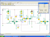
I started solving this problem about 25 years ago by using low tech (transistors, resistors, diodes etc) in the hope that my system could be both simple and cost effective. The stuff on the market is financially crippling. So I designed a control unit consisting of home made PC boards each consisting of a Twin-T block occupancy detector which drives a small reed relay. I like this system because the relay provides total isolation between sub units. The relay contacts provides the Vcc (-18 volts) to an on board diode matrix that drives the signal LEDs. Each PC card has 3M style plugs drive two (east and westbound) signal that can have 3 standard aspects plus two optional ones for sidings etc.

All the PC boards are mounted on a rack and have a standard PC card plug. The configuring is done on the rack's 'backboard'. The output (-18 v) from each board's relay is propogated to four adjacent boards. (two in each direction). This allows for "Halt", "Approach", "Approach Medium" and of course the "Clear" indications. There is also an onboard simple flasher circuit which is used to indicate (Flashing yellow).

My original design was for the American ABS system but the diode matrix is adaptable and can drive any system one choses. I am modeling the old Slovakian steam era signals which use up to five aspects. (Green, single yellow, double yellow and red). A permissive white allows an engine driver to continue past the red for fifty meters for shunting purposes.

When it came to the signals themselves I spent weekends climbing older signals ad taking measurements. I drew up some plans and had the parts etched in brass. The signals are prototypical, to scale, and have that sharp corner crispness so desirable in models.an give me basic instructions on how to add an image (AutoCad maybe) I could forward some diagrams.

Maybe I should try a screen transfer.

Later

Pete
 
Last edited:
several methods to attach a drawing or picture. Easiest method is draw your schematic using one of several free schematic drawing programs. First draw on computer screen then shift/print screen keys. now using MS paint, just paste into MS paint.
Using the little square box, draw around your drawing, copy then hit file/new. hit no when asked to save.
then paste back nto paint, save file as a PNG. then come to this site and attach to your post (manage attachements, submit
OR do same but use a hand drawen schematic and scan into computer.
 
here is a pic of 24 PC boards with 1.27 traces
If you want I can mail you either PULSAR PAPER or boards w/ printed traces on board.
Even etch if you want but you already have chemical.
Let me know as I am doing some boards by the weekend anyway.

Thanks for the offer but being stubborn and wanting to feel that sense of 'I built this myself' I'll have to decline on the offer MrDeb. I've now built two blocks and they work just like they were meant to.

I changed the right angle traces to 45 degree as you said. Just out of curiosity, why is this?

**broken link removed**
 
can open it but where are the LEDs? plus transistors are a fraction the cost of relays.
you schematic is hard to decipher as what are the leds (where?) relays? etc?
download express pcb or draw out the schematic on paper and scan it.
then post it as a PNG file.
indicate all components. still can't see how this circuit you have is better that the one Angi is working on??
IF I could decipher the schematic I could simulate it to see if it works as described.
 
Status
Not open for further replies.

Latest threads

New Articles From Microcontroller Tips

Back
Top