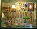
Continue to Site

Welcome to our site!

Electro Tech is an online community (with over 170,000 members) who enjoy talking about and building electronic circuits, projects and gadgets. To participate you need to register. Registration is free. Click here to register now.

  • Welcome to our site! Electro Tech is an online community (with over 170,000 members) who enjoy talking about and building electronic circuits, projects and gadgets. To participate you need to register. Registration is free. Click here to register now.

2nd pcb design program?

Status
Not open for further replies.

Doomguy42

Member
Hi,
I've just produced my first PCB with around 250 holes and I'm so happy with it.
I used express pcb (and express plus for checking).
I'm in the UK so it wasn't viable to produce or ship a prototype over. Express were fantastic, I ordered the basic spec board and they sent me the gerbers. Great service.
I'm planning on a few bigger boards around 1200 holes and I think these will work out very expensive to get the gerbers.
So pricing it up I might be better paying for some software. I have a relatively poor 2014 win 10 laptop which is maxed out on Ram already.
That was my first CAD project, I'm a hobby person but technical enough... I'm hoping to remake old boards instead of repairing battery damage. No Old schematics available ... however I know enough to be able to work out alot of lines from I/Os and I'm seeing the benefits of partially adding a schematic if that makes sense (linking bus lines etc).
Can anyone recommend me a next step software.
Continuity/ trace highlight I can't live without for checking.
Thank You!
 
Absolutely I recommend EasyEDA, which is provided by JLCPCB. Reasons:

1. It is truly easy to use.

2. It is free to use.

3. It's easy to order boards from JLC, but Gerber files are easy to generate and free. They are in the standard form usable by any fab house.

4. The component/symbol libraries are immense. Most parts are included in the libraries, but if the libraries don't include the needed components, it's easy to import Eagle libraries or libraries from vendor library managers.

5. It is cloud-based, but your files are private. As many designs as you like.

6. EasyEDA makes it easy to JLC's free assembly service.
 
I second EasyEDA. Also, unlike previously, there is no charge per hole so when I hand route I never worry about using vias and sometimes use a Manhattan layout.

Mike.
 
When you use the software from a board house the process is very easy. Just hit the "order a board button". In my case I do not want to get stuck with one board house. I have to "plot board files", zip up all the files, send to JLPCB (or anywhere else) then look at JLCPCB's computer to see the results. A little complicated.
I use JLCPCB but with KiCAD, which is also free.
JLPCB, the price is very low but shipping from China to US is $22 for 3 day DHL. I just learned that I can combine orders and get several boards in the same box. Friday I am to get several $5 & $2 boards in the same shipment.
 
Actually, with EasyEDA, it's one click to order boards at JLC.....

Or ONE CLICK to "Generate Gerbers" to generate a zip file ready to send to any fab house. There is zero hassle to create the files to use where you like.

It's far simpler than the process was with my old version of Eagle. Run a separate process to generate the Gerber and drill files, create a zip file and triple-check that all of the necessary files were included, then send the file.

Seems like shipping costs have gone way up recently. I ordered ten boards that are 122mm × 122mm yesterday at JLC. The ten boards were US$16 (more because they were greater than 100mm × 100mm), the stencil was US$7, and shipping was US$35, using "Global International" which claims 1 – 2 week service. DHL was about $10 higher.
 
When you use the software from a board house the process is very easy. Just hit the "order a board button". In my case I do not want to get stuck with one board house. I have to "plot board files", zip up all the files, send to JLPCB (or anywhere else) then look at JLCPCB's computer to see the results. A little complicated.
I use JLCPCB but with KiCAD, which is also free.
JLPCB, the price is very low but shipping from China to US is $22 for 3 day DHL. I just learned that I can combine orders and get several boards in the same box. Friday I am to get several $5 & $2 boards in the same shipment.

I had some come Monday (well I didn't, as I'm on holiday, but I got the email that they had been delivered), the postage was £156 or so, plus more than £50 VAT - the postage depends on weight, so it's OK if you're ordering small quantities of small boards.

A few days later I ordered some larger boards (for me - but through work :D ), and just the standard set of five. I noticed that there's now a much cheaper (but much longer) postage option (10-12 days), so as I was going to be away I used that instead of DHL. Be interesting to see how long they take.

Edit:

Just checked the tracking, anyone make any sense of this?.

Shipment Tracking
  • 2022-08-10 14:53:07
    Departed from facility
  • 2022-08-08 10:15:56
    Processed at facility
  • 2022-08-06 13:53:00
    Arrived at origin facility
  • 2022-08-04 12:46:27
    Shipment data received - Awaiting Parcel Handover to DHL
  • 2022-08-04 04:00:01
    Data Submitted - Awaiting Parcel Handover to DHL
  • 2022-08-05 12:48:08
    Packaged,waiting for pick up by the carrier,Tracking #: HKBCQ2022080411412093895
 
With any of the programs is it possible to import an image to use as a template?

I'm looking at the damged board I want to remake and if I strip it and scan it as an image. I was wondering can I import an image to use behind for tracking and checking I don't miss anything? Might make it quicker too than measuring everything with out with verniers when positioning?
 
Unless it's very simple it's not easy to create an exact copy. Many parts may no longer be available as through hole components. It's normally better to work out a schematic and work from that. The most important parts, for compatibility, are the connectors.

If you post a picture of both sides of the board, some members here are very good at working out a schematic.

As an example, I remade a board from the 90s that was originally 150x100 mm and the new one was 50 x 25. Things have changed huge amount in the last 30(maybe 40) years. Do you know when this board was produced?

Mike.
Edit, the function of the board is another factor. High frequencies can require particular layouts.
 
Hi Mike,
Yes it's around 92. It's a z80 cpu, plenty of z80 pio ics, it's large around A4 sheet of paper size. It's pretty much an arcade pcb style board. Lots of the components are obsolete... but that's where the fun is right? OK no-but I couldn't even solder a few years back and I'm really enjoying pushing myself...so why not?


To keep learning I know I need to get better with developing schematics and component selection so my plan is to draw out a few of the circuits like reset, voltage reference, clocks as a schematic and look for modern components like surface mount logic ics and transistors.

I'm an electronics hobby person so my approach might be slightly different to a proper engineer, I've not studied electronics so I only have about 4years hobby experience.

From a cad/design point of view I'm confident I can do it... but I'm mechanically looking at it. Before I start I'm just considering any ways to make it easier so an image imported to trace over really would help if it's possible or anything like that?

.
 
Old boards like Arcade boards from the 90s (probably earlier) are often routed using a Manhattan routing scheme - google Manhattan routing. If you can get the components, draw a schematic, layout the board so the component (and particularly connectors) are the same then it would be easy to use a Manhattan technique to route it.

Does your board contain any ROM? If so, do you have the code that they contain? Some ROM images are available from the https://www.gamesdatabase.org/.

Mike.
Edit, Wow, on that database I just found Crazy Balloons. That was the first game I wrote (copied) for the Spectrum back in 1983.
Edit2, in that era, many manuals contained schematics. Might be worth a search. I have a Monster Bach Pinball machine and the manual contains a full schematic - even in 1998. However, even back in 1998 they had ASIC (Application Specific Integrated Circuits) chips which are (pretty much) impossible to replicate.
 
Last edited:
Hi, yes you are totally correct it's a Manhattan routing system... I always called them as under over boards!

Here's a pic attached... this isn't the exact board I will do with the daughter board but it's pretty much the same.
My design spec-
Perimeter the same
All input output connectors the same
64way 41612 connector same place.
The drive areas pretty much need to be the same and close by to the corresponding connectors.

The rom sets are common and I have a programmer. Unfortunately no schematics but on the plus side there's nothing like asic or custom logic.

If you have been working on z80 boards since 83 I would be glad for anything you can teach me or have any pointers.

I'm coin op mad... I love what old junk you can buy cheaply and fix up. I'm actually a high end cabinet maker/joiner so restoring old machines is no problem. My hobby has spanned into board repairs and now pcb design. Because I don't have an electronics background the route of scanning a board and importing the image to the pcb design program was attractive because I can place so many connectors and components easily... if it's possible?

Also included a vid of my first board I've built (purple one) which was a small trial.
You can see the electronics involved is arcade but it's slightly different with stepper motor drives, opto sensor, lamping etc. I was literally over the moon with it.
Lowered the quality to try and post it.


Attachments

  • 20220817_204316418.jpg
    20220817_204316418.jpg
    2 MB · Views: 190
Status
Not open for further replies.

Latest threads

New Articles From Microcontroller Tips

Back
Top