Continue to Site

Welcome to our site!

Electro Tech is an online community (with over 170,000 members) who enjoy talking about and building electronic circuits, projects and gadgets. To participate you need to register. Registration is free. Click here to register now.

  • Welcome to our site! Electro Tech is an online community (with over 170,000 members) who enjoy talking about and building electronic circuits, projects and gadgets. To participate you need to register. Registration is free. Click here to register now.

Switched Capacitor Integrator

Status
Not open for further replies.
Hello again,

Ok great. Just to be clear, i am getting now from an external source that the 'gain' being referred to here is NOT the open loop gain after all, but is some other gain yet to be disclosed. I think now it is the gain of the RC integrator itself, but we'll see.

Wizard, now that you have simulated the two circuits i would like to see two things:
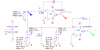
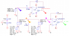
1. The two circuits and all component values.
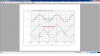
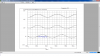
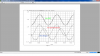
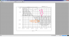
2. The two simulation waveforms, one from each circuit at least.
3. How you are reasoning that the two are the same, or are related by that formula in the thread.

Ok that's three things :)

Hi Al,

Please bear in mind that the main problem which the main formula is going to explain and cover is that when we design the Continuous integrator and use the related formulas (I'll rewrite them in the next post) to design the equivalent SC one we end up with a SC integrator that its gain is not similar to the Continuous one (as you'll see in the waveforms in my next post)... The main formula refers and talks about such situation and shows (or at least tries to show) us the relationship of these 2 integrators at such state...

Ok please let me write my next post and show the schematic and the waveforms of my design...
 
First we suppose that we have been told to design a continuous integrator which can work at input frequency of 25KHz, and then design the equivalent SC integrator...
(I suppose that a sampling frequency of 40 times the input frequency would be acceptable when I go to design the SC integrator... )

A. Designing the continuous integrator:
1. Ok we ourselves define the C2 value and then find the R and C1 using the following formulas.
I define the: C2=1nF.
2. Now we find the value of "R" using this formula:
R=1/(Fin*2pi*C2) -> R=1/(25KHz * 2pi * 1nF) = 6.366k

I used the above formula to find the value of R with respect to the input frequency and C2 to guaranties that our continuous continuous integrator will have gain=1 at our input frequency.


B. Ok Now we go to design the SC Integrator (We here are going to design the equivalent SC integrator):
3:We use the below formula to find the value of the "C1":
C1= T/R = 1/(Fclk * R)

As I said I consider the sampling frequency to be at least 40 times higher than the input frequency --so a sampling frequency of 1MHz would be a good choice.
So:
C1=1/(1MHz * 6.366k) =0.157pF

Now we have everything which we need to design our SC integrator too:
C2 (SC)=1nF (C2 value is the same for both the continuous and the SC integrators)
C1=0.157nF
Fin=25kHz
Fclock=1MHz


OK, with respect to the said values in this post, I'll show you the schematics of both continuous and SC integratos which I have designed and the input/output waveforms...
 
Last edited:
- I have used the PSPICE simulator to design the integrators here...
- As you see I have used the TL072 op-amp here for this design...
- As you see in the schematic, the input frequency is 1Vp (2Vp-p) here.

- If you take a look at the waveforms you'll see that it clearly shows the gain of the continuous integrator to be 1 ( ie Vo continuous /Vin =1)
- Now Please take a look at the output waveform of the SC integrator there... It shows that the Vout for the SC integrator is equal to almost 1.8Vp-p
So its gain would be:

Vo sc/Vin = 1.8/2 = "0.9"

Here's the main formula which we were and are talking about here:

(0.5* (C2/(C2+C1))* (CONTINUOUS INTEGRATOR GAIN AT INPUT FREQUENCY)
As we noticed the gain of the continuous integrator here is 1
So the gain formula for the SC integrator with respect to the gain of the Continuous one would be:
(0.5* (C2/(C2+C1))

We had:
C2=1nF
C1=0.157nF


Using the main formula (ignoring the "0.5") We see that the gain of the SC integrator would be: (C2/(C2+C1) = 1/1.157 = "0.86" which is so close to "0.9" we found through the waveform.

So the main formula is going to tell us the relationship between the gain of the continuous integrator and the SC one... It says that the gain of the SC integrator won't be exactly equal to the gain of the equivalent continuous one.....
 

Attachments

  • for eto schematic.png
    for eto schematic.png
    27.2 KB · Views: 322
  • waveform For eto.png
    waveform For eto.png
    61.8 KB · Views: 329
Last edited:
Hello again Wizard,

That's very good. With this new post you have just made this concept a LOT more interesting, but you still have a little more work to do.

Note that when we have an amplifier with a gain say G, the output is proportional to the gain G as:
Vout=G*Vin

This is a very simple concept, i am just spelling everything out to be clear.

This means that if G=5 and Vin=1 we get:
Vout=G*Vin=5*1=5

but if Vin=2 we get:
Vout=G*Vin=5*2=10

So the main point here is that G holds for both inputs, 1v and 2v, and if we have two gains G1 and G2 that we believe are the same, then we would have:
Vout1=G1*Vin
and
Vout2=G2*Vin

and with G1=G2 we would always have:
Vout1=Vout2

no matter what we choose for Vin (within reason).

To to prove that G1=G2 we must show more than one result for two different Vin's, and this means we need to show two different simulations but without changing anything except the value for Vin. (Note more than two would be even better as two alone could still coincide with a parabolic behavior while with three that would be very difficult to stumble on by accident).

So you have to change Vin to some other value that is significantly different than it was for the first run, and then do a second run, at the very least. If you wanted to you could do a stepping of Vin over several different values and if the output of the two circuits agree, then i think you would have proved that the two are equivalent. However, doing one single simulation with only one value for Vin does not prove anything except that you can set the gain to be the same for one value of Vin :)

So do a couple more simulations with different Vin and hopefully you can prove this once and for all. I am interested to see the results also.

One more small note...
You also have to be careful that some feature of one of the models and/or the values for the components dont dominate the response. If this occurs then the feature we are looking for will never show itself. For example, if you are designing a low pass filter with cutoff 1.2kHz and you follow it with a low pass filter with cutoff 1kHz, it might look like the 1.2kHz filter is working when really it could just be a single straight piece of wire with the 1kHz filter doing all the work. If you look closer you will find the response doesnt follow the right pattern, but it may take very accurate values to see it. If the values are chosen so that they do not force behavior that coincides with other behaviors, then it will be easy to see.
For this reason the Vin test values should be significantly different but the capacitors should be chosen so that the expression with the capacitors comes out significantly different than a reduced complexity expression such as C2/C2 for example, or worse yet, C1/C2 (although i doubt this can happen too easily).


Hi Al,

I am also glad that it seems to work (at least till now)... And we seem to be more close to the main formula than ever!:)....
The waveform also nicely shows that it integrates the input signal at 90 degree too (for both the Continuous and the SC integrators) which is perfect...

OK I did a couple more tests for you with Vin = 0.8Vp-p and Vin=3Vp-p (I'll add the waveforms for your judge in my next post)...
If you need more tests to be done by me or would like to see the wavform or the amplitude of every other point of the circuit please just let me know:)...
I myself would like to show you the waveforms at the outputs of the switches (S1 & S2) too, and will do that soon..

Regarding your last paragraph... I wanted one of my friends here to do a simulation test using HSPICE software... I wanted him to select the values for all the components just exactly the same as what I chose in my post #26... We reached to the same result which is very Promising....
Anyway, Al, there is a huge difference between (C1/C2) as thought before and (C2/(C2+C1)) for the gain if you know what I mean?
 
Ok, SO we had C2=1nF, C1=0.157nF, Fin=25KHz and Fclk=1MHz...

In my post #43, we saw the waveforms when the input is 2Vp-p.
Now Please take a look at the below waveforms when the input is 0.8Vp-p and then 3Vp-p... (the formula (C2/(C1+C2) still holds here)...
C2/(C1+C2) -> 1/(1+0.15) = 0.864 --so simply multiply the input voltage by 0.864 to reach to the Vo (SC) and then take a look at the waveforms--
 

Attachments

  • vin (0.8vp-p).png
    vin (0.8vp-p).png
    62.2 KB · Views: 331
  • vin (3vp-p).png
    vin (3vp-p).png
    63.7 KB · Views: 341
As I mentioned before I am going to add the waveforms at Switch points too (I have called those points as "A" and "B" in the below schematic)...
Please keep in mind that the schematic here is the exact schematic of post #43 (the input voltage is 2Vp-p).
 

Attachments

  • second schematicfor eto.png
    second schematicfor eto.png
    28.3 KB · Views: 332
  • A & B points.png
    A & B points.png
    76 KB · Views: 321
  • A & B points (colourful).png
    A & B points (colourful).png
    37.9 KB · Views: 317
Hello again,

Ok so we are seeing some correlation here, but i do note that the output of the SC is lower than the Continuous integrator. Perhaps you should investigate that.
Also, according to the formula it does not obey C2/(C1+C2) it is supposed to obey 0.5*C2/(C1+C2), so what is going on?

Another idea would be to make the small capacitor larger and see if it still works. We would like to see some indication of the sensitivity to component variation to make sure we havent chosen values that just happen to work when other values dont work.

Also, did you do a calculation to make sure the op amp itself is not influencing the signal at the chosen frequency? 25kHz seems ok i guess, but 5kHz would be even better even if you have to lower the input signal levels for the test. Also, 1us for the clock may be too fast for the op amp too, so maybe 100kHz would be better for that, even if you have to lower the input test frequency.
100kHz/50=2kHz test frequency, which would mean a 2kHz input and 100kHz clock.

Thanks for your input Al,

Well we are going to reach to the correct formula or relationship for this circuit, whether it gets a "0.5" or not... As you see we are going to use the simulation to find the real relationship and then go to why that relationship holds (ie the mathematics)... For now I myself assume that the formula might not have a 0.5 (according to my simulation), and assume that maybe that "0.5" was there due to a misunderstanding of the calculating the gain using the Vinp-p and Vop... ie Vop/Vinp-p.

Yes I know what you mean... So please let me know which values you prefer for C2, R, C1, Fin,Vin and Fclk? I will do a test with the values you give to me and will back to you ASAP.

I had a test to see if the gain of the op-amp changes when the input signal is 1MHz. To do this test, I simply connected a 1MHz signal ---once the signal was square and once it was a sine wave- to the continuous OP-AMP, the gain was hold at 1 for this frequency too, so I came to the conclusion that the op-amp I have chosen seems to be ok to work up to 1MHz...
 
Last edited:
I forgot to mention Al, please select the values you are going to give to me they way that our circuit takes the integration at 90 degree.

Thanks.
 
Al, do you think that you can try to come up with a simulation too with your simulator? Or at least try to simulate the switch cap itself as a resistor and connect its output to say another real resistor and see the wave-forms and amplitudes like a voltage divider?
Req = 1/(Fclk*C1).... so if Fclk=1MHz and C1=0.157n then the Req would be 6.36K. I believe if we connect the Switch cap to anther 6.36K resistor then the amplitude would be exactly 1/2 at the joint point of the two... Are you agree? the rest of the circuit is exactly the same as the continuous one...

But if you think that you can come up with the whole circuit, then please keep in mind that the formulas which I wrote to reach to the values for R and C1 (and somewhat the 1 to 40 ratio for Fin and Fclk) are important here cause they are related to each other...

Thanks.
 
Last edited:
Al, do you think that you can try to come up with a simulation too with your simulator? Or at least try to simulate the switch cap itself as a resistor and connect its output to say another real resistor and see the wave-forms and amplitudes like a voltage divider?
Req = 1/(Fclk*C1).... so if Fclk=1MHz and C1=0.157n then the Req would be 6.36K. I believe if we connect the Switch cap to anther 6.36K resistor then the amplitude would be exactly 1/2 at the joint point of the two... Are you agree? the rest of the circuit is exactly the same as the continuous one...

But if you think that you can come up with the whole circuit, then please keep in mind that the formulas which I wrote to reach to the values for R and C1 (and somewhat the 1 to 40 ratio for Fin and Fclk) are important here cause they are related to each other...

Thanks.

Hi,

I am not sure what you want to do here.

What i was suggesting, more or less, is that you change capacitor values and note that the circuit follows C2/(C1+C2).

So if you have gain Gc=C2/(C1+C2) and you change C2, then the simulation should reflect that change in gain. For simple example, say C1=1 and C2=1, then we have:
Gc=(1/2)=0.5
and lets say the output with 1v peak ac input is 3 volts peak for the SC integrator.
Then if you change C1 to 3, then the gain changes to:
Gc=C2/(C1+C2)=1/(4)=0.25
so the output should change to 1.5 volts peak for the SC integrator.

Dont you agree that this relationship should hold?
 
Hello again,

I thought i should mention also that you may be wanting to hold C1 and C2 constant after the calculation, which would then be a different story. That would make the gain constant and not be able to change:
Gain=0.5*C2/(C1+C2)

which after the continuous integrator values are chosen then the two capacitor values are calculated from that, and then we can apply the gain C2/(C1+C2). The only thing we would be missing then is the "0.5" which still doesnt fit in.

One thing i have been meaning to mention from day 1 and kept forgetting and forgetting to mention, probably because we were talking about more specific stuff all the while and i have other home issues going on...is the general method for linearizing a switching circuit. There is a general method for converting a switching circuit into a linear circuit, which takes into account several things. I think you should investigate this. It is often used for buck circuits and boost circuits alike. The circuits are turned into linear circuits so that the overall behavior (like stability) can be estimated without having to analyze every single switch action and it's effect on the output. We loose the instantaneous values like what we see as ripple due to the switch action on and off, but we gain a faster calculation of the stability criteria.

I'll have to try to find this method and post a link or something. It's a wonderful method and if the linearized gain of the SC integrator is some set value then this general method will find it. I cant believe i forgot to mention this so many times. Must be getting too old :)

I'll check around for it again.
BTW it is a matrix method, starting out from the state vector differential equation of the circuit. The result is sometimes called the State Space Averaged Model.

Here is a quick snapshot of the equations involved in this method...
 

Attachments

  • LinearStateSpaceEquations-1.gif
    LinearStateSpaceEquations-1.gif
    9.7 KB · Views: 300
Last edited:
Status
Not open for further replies.

Latest threads

Back
Top