Strange one here!
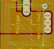
I've using a MCU which is 3 adc channels short, so I added 6x NMOS and 1x PMOS to switch the channels. In all cases I'm measuring either current over a resistor or voltage by a divider. The drive voltage is 3.6v (ignore the 3V0).

To prevent leakage through the alternative turned off nmos the voltage I found has to be kept below 0.4v as once it heads towards the 0.7v point there's enough leakage to make a difference to the read. The voltages and the current levels are all below 0.4v so the 3.6v drive comfortably turns on the 2N7002 NMOS.
The voltages are bang on, no problem there. Now, when reading the current over a 200mOhm resistor, 125mA the read is perfectly correct. Increase to 500mA, still correct. Grand!
However when using a 100mOhm resistor then the read is amplified. At 250mA the read is x1.2 larger. This increases so that mathematically it's something like [x1.4 - 50]
I measured the output at the resistor and it's correct, and then again at usbADC and it's definitely higher. My only thought was there's still some leakage through the NMOS, enough for the ADC to capture, so I turned on the MCU's 15k pull-down on the pin. It made no difference.
Any other thoughts?
Cheers!
Andrew
I've using a MCU which is 3 adc channels short, so I added 6x NMOS and 1x PMOS to switch the channels. In all cases I'm measuring either current over a resistor or voltage by a divider. The drive voltage is 3.6v (ignore the 3V0).
To prevent leakage through the alternative turned off nmos the voltage I found has to be kept below 0.4v as once it heads towards the 0.7v point there's enough leakage to make a difference to the read. The voltages and the current levels are all below 0.4v so the 3.6v drive comfortably turns on the 2N7002 NMOS.
The voltages are bang on, no problem there. Now, when reading the current over a 200mOhm resistor, 125mA the read is perfectly correct. Increase to 500mA, still correct. Grand!
However when using a 100mOhm resistor then the read is amplified. At 250mA the read is x1.2 larger. This increases so that mathematically it's something like [x1.4 - 50]
I measured the output at the resistor and it's correct, and then again at usbADC and it's definitely higher. My only thought was there's still some leakage through the NMOS, enough for the ADC to capture, so I turned on the MCU's 15k pull-down on the pin. It made no difference.
Any other thoughts?
Cheers!
Andrew