Continue to Site

Welcome to our site!

Electro Tech is an online community (with over 170,000 members) who enjoy talking about and building electronic circuits, projects and gadgets. To participate you need to register. Registration is free. Click here to register now.

  • Welcome to our site! Electro Tech is an online community (with over 170,000 members) who enjoy talking about and building electronic circuits, projects and gadgets. To participate you need to register. Registration is free. Click here to register now.

Rookie needs help to understand why his A-class amplifier doesnt work (measurements and schematic attached)

GreenGecko7

New Member
Dear all, nice to meet you !

I recently invested in some tools to build amplifiers (my first oscilloscope + all-rounder C and R kits.). My end goal is to build an AM radio.
I have some basic knowledge in electronics : I have studied transistors and OP Amp functioning during my college masters degree. I also have a few Arduino projects under my belt.

However my 2 last tries at building a functiuning Class A amplifier failed. I need some help to understand why !
I based the diagram on this famous video :
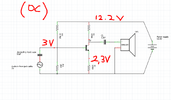
And I adapted the values to fit my 12.2V switch-mode power supply.

Attached the schematic, in red are the DC measurements made via oscilloscope/multimeter.
Also, no AC component survives the first capacitor : the oscilloscope probing remains flat at +3V DC (DC coupling) when probed on the transistor base with reference on the ground.

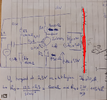
Can you help me understand what fails, and suggest me fixes?
I can probe additionnal points if you tell me what to look for specifically.

Thanks a lot in advance ! :)

Benjamin, from France
 

Attachments

  • Circuit class A as made with measurements.PNG
    Circuit class A as made with measurements.PNG
    104.8 KB · Views: 93
Well it's a really crappy circuit, and will provide hardly any power output at all, and is massively inefficient as well. But if you've got no signal on the base of the transistor, yet you have on the input of the capacitor, then you've got something connected wrongly, or a component is faulty.

I presume you've built it on a breadboard?, these are notorious for poor connections, so check for signal on the actual wires - on both sides of the input capacitor, and if you get signal on both of those, then try on the two biasing resistors, again on the actual wires.

You're also missing an essential component, which is a decoupling capacitor across the supply rails, stick a 47uF or a 100uF across it.
 
The transistor is saturated, The voltage on the base of the transistor is higher than it should be when calculated from the values shown for R3 and R4 and the supply voltage. If you check the voltage on the collector of the transistor you will find that is not much higher than the voltage on the emitter.. I think the value of R3 or R4 is not the same as shown on your schematic.
Even if the biasing was correct it would only have a voltage gain 4.7 but with a 15 ohm speaker connected the voltage gain would be about 15/1000 = 0.015. (So it would be an attenuater not an amplifier.

Les.
 
Hello Nigel, thanks for the first reply !

I soldered the connexions indeed : I'm not a fan of breadbords when it comes to small-signal due to poor connections as you mentioned.

I'll consider adding a capacitor in parallel in between +VCC and GND. Though for now, in the prototyping stage, it is not a "hard" requirement, is it?

Hello Les Jones !

You were right. I investigated this matter about an hour ago because I, too, believed the base current was too high and the transistor, saturated. So I changed R3 and R4 to both 47kOhm, and good news : now my AC signal shows up on the base ! I measured U_base = 2.6V DC +- 0.3V AC (x10 probe, so... 26VDC + 3VAC? Strange :/ ) Edit : wrong configuration of probe multiplier setting on the scope.
Also I made a mistake regarding the input decoupling capa : it is 100nF and not 10uF as shown on the graph. Anyway, signal flows through.

Now the issue is, there is close to no power on the output. Did I choose my transistor wrong? (BD135, gain of 25 to 250 according to datasheet). Should I review the circuit design, and if so, how?

New measures : The voltages (DC coupling, x10 probe) were 3.8V DC +-0.15V DC at the collector, right between the transistor and the outpout capacitor. Why such a small variaton? I'm surprised because those tensions were measured with the X10 probe, that would mean I had 38VDC +-15VAC on my probing point? surprising.. How would you explain this, you, experienced members?

Best regards,

Benjamin
 
Last edited:
Hello Dana, thanks for the schematic. Interesting and smart to model the speaker as RL in series, i would not have thought of it.
Are C3, C4, R5 and L1 part of the speaker model or are they a mean to stabilize the reference potential?
 
Hello Nigel, thanks for the first reply !

I soldered the connexions indeed : I'm not a fan of breadbords when it comes to small-signal due to poor connections as you mentioned.

I'll consider adding a capacitor in parallel in between +VCC and GND. Though for now, in the prototyping stage, it is not a "hard" requirement, is it?

Yes it is, the entire circuit works on the basis that the supply rails are at the same AC potential.

Hello Les Jones !

You were right. I investigated this matter about an hour ago because I, too, believed the base current was too high and the transistor, saturated. So I changed R3 and R4 to both 47kOhm, and good news : now my AC signal shows up on the base ! I measured U_base = 2.6V DC +- 0.3V AC (x10 probe, so... 26VDC + 3VAC? Strange :/ )
Also I made a mistake regarding the input decoupling capa : it is 100nF and not 10uF as shown on the graph. Anyway, signal flows through.

Now the issue is, there is close to no power on the output. Did I choose my transistor wrong? (BD135, gain of 25 to 250 according to datasheet). Should I review the circuit design, and if so, how?

New measures : The voltages (DC coupling, x10 probe) were 3.8V DC +-0.15V DC at the collector, right between the transistor and the outpout capacitor. Why such a small variaton? I'm surprised because those tensions were measured with the X10 probe, that would mean I had 38VDC +-15VAC on my probing point? surprising.. How would you explain this, you, experienced members?

Best regards,

Benjamin
It's still an entirely non-practical amplifier, and doesn't even amplify at all anyway - it's just an attenuator. If you're wanting an amplifier, then build a proper one, one that works.
 
I don't understand your reasoning in changing R3 and R4 to 47K. The original values should have given about
12.2V x 1K/(1K+4.7K) = 12.2V x 1K/5.7K = 2.14 volts. In practice it would be a bit less than this due to the base current. The value of these resistors is chosen so the base current does NOT change the voltage on the base very much. Choosing equal values means you were seting the base voltage to 6.1 volts but choosing higher values meant that the base current had more effect in dropping the voltage. Did you measure the values of R3 and R4 to find out why you had 3 volts when the calculation predicted 2.14 volts. I agree with the other comment about it being a very poor design.

Les.
 
Nigel, got it, I'll add a capa inbetween +VCC and GND just for good measure and eliminate this potential issue. Doesnt cost much.

I agree, this is a very simple and inefficient amplifier (or as you call it, attenuator indeed). But I don't get why I dont see swings from 1V to 11V as expected. Is my base current too weak ?

As per the design itself, should I try again with a higher gain transistor as shown attached, or should i go directly to builing a class-AB amp? (i have symmetrical supply if required).

I must say I wanted to build specifically a class A amp, because I believe these would have made good first-stage amplification for low signals straight out of the antenna in my (future) AM radio.

Edit : added atttachement : new scheme with 2n3904, hfe=100 @Ic=2mA
 

Attachments

  • schema elec v3.PNG
    schema elec v3.PNG
    697.7 KB · Views: 65
Last edited:
Les Jones,

I had a feeling something was off with the bias resistors and the base current was too high causing transistor saturation, so I decided to reduce bias current by a factor 10, hence the change of R3 from 4.7 kOhm to 47 kOhm.
To keep a bias way above 2V, i also changed R4 to 47 kOhm.

I did not take the individual values of R3 and R4 before modification, this would have been valuable information though.

It seems that at the moment the bias voltage is set by R3, V_be and R2 rather than R3 and R4, right?
Current can flow too easily through base at the moment, maybe i need to lower R4 to come closer to (U_R2 + 0.7V) ?
 
Hey all,

So I rebuilt the circuit mentioned above and it works, but still outputs less power than the input.

I have

Input (sine wave via phone) = 0VDC +- 0.4VAC
U_b =2.3V +-0.4V
Output on load : 0.1VDC +-1.15VAC
Probing directly on collector : 6.9VDC +- 1.1VAC

So, again, the swing is only 2.2V peak to peak. Any ideas on how to improve it? Also, the output power is ridiculously quiet compared to the power i get by plugging my phone directly to the speaker. Any ideas?

It's late here, I'll come back tomorrow to maybe gather your insight. I'll also give a shot at a class AB tomorrow... probably.


Good afternoon,

Benjamin
 
Hello Dana, thanks for the schematic. Interesting and smart to model the speaker as RL in series, i would not have thought of it.
Are C3, C4, R5 and L1 part of the speaker model or are they a mean to stabilize the reference potential?
Yes all the components below the text Speaker Model are part of the model.


So, again, the swing is only 2.2V peak to peak. Any ideas on how to improve it? Also, the output power is ridiculously quiet compared to the power i get by plugging my phone directly to the speaker. Any ideas?

The issue is you are trying to drive a very low Z load. That in turn means lots of current in the transistor
driven by need to lower its collector and emitter Rs. Its a cat chasing its tail, as you try to do this, Class A,
the Pdiss of the transistor rises quickly.


Regards, Dana.
 
Class A means the load has a constant DC bias current with AC swing on the collector.

The collector DC pullup current must be greater than the AC load current otherwise the collector collapses into saturation as a null voltage gain switch rather than the typical voltage gain of Rc/Re of an emitter current-controlled current sink at the NPN collector.

Class A is not practical for a speaker as the DC current and if AC coupled, for the same reason, the collector resistor, Rc must be less than the Load R.
 
I had a feeling something was off with the bias resistors and the base current was too high causing transistor saturation, so I decided to reduce bias current by a factor 10, hence the change of R3 from 4.7 kOhm to 47 kOhm.
To keep a bias way above 2V, i also changed R4 to 47 kOhm.

With 100 Ohm emitter resistor and 470 Ohm load, the voltage across the collector resistor will be approx. 5x that across the emitter resistor.

2V across the emitter on means 10V across the collector one, taking the entire 12V supply and the transistor pretty much hard on!

The bias should put the collector voltage near the middle of it's practical range; somewhere around 7V (~5V across the collector resistor).

That needs about 1V across the emitter resistor, so ~1.6V base bias.

I did a video on calculating bias a whole ago, here:

 
Hello Diver300,

The speaker resistance is 3.5 ohm (measured). So the official impedamce must be 4 ohm.

Hope that helps
I think that others have said this in different ways. The circuit you have has a 470 Ohm pull-up resistor. It can't provide enough current to drive that speaker with a large amplitude. That is why there isn't much output amplitude.

If you reduce the resistor a lot so that it can drive a low impedance speaker harder, it will use a lot of current even when there is nothing being amplified. This is why class-A amplifiers aren't used much.

The alternative is to have a transformer to drive the speaker. I don't actually recommend that, as a different type of amplifier would be much easier to make than a transformer.
 
I must say I wanted to build specifically a class A amp, because I believe these would have made good first-stage amplification for low signals straight out of the antenna in my (future) AM radio.

Note that such an amplifier is not generally suitable as-if for RF applications - you really need at least some form of bandpass filter or tuned circuit before that, otherwise it will try to amplify any signal at any frequency, which can usually resulting in distortion, overload and intermodulation etc.

Most of the simple receiver circuits on the internet either only work with strong local signals, don't provide enough details to reproduce them, or just don't work at all!

Most commercially made (and serious amateur project receivers) use a superheterodyne system, as that is the simplest approach to getting both good selectivity and high sensitivity.

That is a rather complex system for someone inexperienced in building electronics.

Have a look at a superheterodyne kit such as this for an example of the requirements - this is dual band, so one RF section (upper?) is for medium wave & the other is for FM, with the audio section at the centre right.


(The required IF transformers etc. are getting very hard to obtain, so such as that with full sets is not a bad parts source even if you did not built it on their PCB).

I'm not trying to put you off, just hoping to help you avoid the frustration of dead-end designs!
 
Hi all,

Thanks Dana, Tony and Diver. It seems obvious now that you point it out : i can't expect high output current with resistors in series in between the supply voltage and the laod. So this design IS indeed doomed to be a low output impedance one, not what I was looking for !

(Thanks for the informative resource, Dana)

Damn rjenkinsgb, your video is very complete, thanks for your time and for sharing ! I'll try to modify my bias resistors to stabilizer V_collector at 7 volts and see if it helps with my output voltage. I won't connect any load, and will just try to get some tension gain out of this design. Also, I love the idea to add a R+C in parallel of R2 to decrease impedance, simple but efficient !
 
Hello Rjenkinsgb,

I totally agree, this amp part is only one stage fo the multiple ones needed to build a RF emitter. I had in mind to build, separately, an RF oscillator around 29MHz, amplify it with low distorsion to get good output impedance (hence aiming at class A in the 1st place), run it through a multiplier and finally send the composite signal to the power amplifier.

It is, indeed, ambitious, and too much to bite at once that's why I decided to cut the building into several sub-builds that can be tested independently. I'm definitely not qualified enough to design my own circuits (goal is to get some knowledge about it though), but have studied electronics in my degree and always liked it. That allows me to understand explanations like the ones in your video ;)

I'm not a fan of premade kits with PCBs because you don't learn about what's actually happening in my opinion. But getting one to scavenge parts and maybe follow a simpler, less efficient yet understandable layout sounds great. I'll have a look at

And I agree with you, internet is full of schemes and unreliable info (I see it in my own expertise domain), so I can understand a good part of the online "simple schemes" are not functionnal.

Where would you suggest for me to find "easy" and reliable schemes?
By easy, I am thinking of less than 20 individual components to fit together and get a working stage to be later integrated in my AM radio model.
 

Latest threads

New Articles From Microcontroller Tips

Back
Top