earckens
Member
Hi spec and Les,
I studied all the ideas of the last few hours and have a few questions, just to confirm before I start building tomorrow (and spec: I promise not to wait until the prototype is ready and finished, I try to start on the Eagle drawing tomorrow):
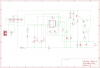
I refer to the drawings in post 113 and 119:
1. I miss the voltage feedback circuit to -comp:
a. no need to recalculate the voltage divider 18k / 82k?
b. value for the voltage regulator pot: remains at the original 2k2?
c. maximum 46V gets fed back to -comp via the 82k resistor: +comp remains unchanged compared to the original circuit; surely this is not right?
2. 18V zener regulator: currently based on 40mA (both zener bias and total load for 18V).
a. Is this sufficient?
b. Why 18V and not for example 30V? 36V?
c. Why not a series regulator with a transistor? (if it can be solved with a zener, sure why not?)
Thanks a lot!!
Erik
I studied all the ideas of the last few hours and have a few questions, just to confirm before I start building tomorrow (and spec: I promise not to wait until the prototype is ready and finished, I try to start on the Eagle drawing tomorrow):
I refer to the drawings in post 113 and 119:
1. I miss the voltage feedback circuit to -comp:
a. no need to recalculate the voltage divider 18k / 82k?
b. value for the voltage regulator pot: remains at the original 2k2?
c. maximum 46V gets fed back to -comp via the 82k resistor: +comp remains unchanged compared to the original circuit; surely this is not right?
2. 18V zener regulator: currently based on 40mA (both zener bias and total load for 18V).
a. Is this sufficient?
b. Why 18V and not for example 30V? 36V?
c. Why not a series regulator with a transistor? (if it can be solved with a zener, sure why not?)
Thanks a lot!!
Erik
")