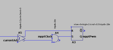
I find myself doing this quite often and have occasionally wondered if there's a latch that can perform the same behaviour of the AND gate and SR.
SR - possible SR=1 violation
D - only actions on the clock
JR - don't want the toggle behaviour
The only thing I can think of is using 4 NAND gates to do the SR gate then using a pull-up on the second input of the S input (which is normally hidden) with a weak pull-up.
SR - possible SR=1 violation
D - only actions on the clock
JR - don't want the toggle behaviour
The only thing I can think of is using 4 NAND gates to do the SR gate then using a pull-up on the second input of the S input (which is normally hidden) with a weak pull-up.
")
