Continue to Site

Welcome to our site!

Electro Tech is an online community (with over 170,000 members) who enjoy talking about and building electronic circuits, projects and gadgets. To participate you need to register. Registration is free. Click here to register now.

  • Welcome to our site! Electro Tech is an online community (with over 170,000 members) who enjoy talking about and building electronic circuits, projects and gadgets. To participate you need to register. Registration is free. Click here to register now.

Input impedance of self-biased stage

Status
Not open for further replies.

hanhan

Member
Hi,
Please help me with this question about self-biased stage of MOSFET.
self-biased-stage-jpg.80782

Here is the answer that I saw in another forum:
Even though there is no voltage drop across RG, it still conveys a voltage to the transistor's gate. If you remove RG, then the gate is floating.

So why not make RG zero ohms? That will also convey the voltage to the gate. However, it will create a low impedance for a signal that is applied to the gate, which will then just be RD ohms away from an AC ground at VDD.

We need a resistor to help maintain whatever input impedance is necessary at the gate.

If you look at the DC picture, it goes something like this. Initially, no current flows through the transistor and so the drain is at VDD. If the drain is at VDD, that means that the gate is also at VDD. But if that's the case, the transistor is actually turned on and so current flows, causing a voltage drop on RD. But, aha, we have feedback! If current flows through RD, then the drain is not in fact at VDD and therefore neither is the gate, so the transistor is not quite as turned on as we thought. The solution to this feedback loop is the operating point, and as you can see, RG is very much involved in it.
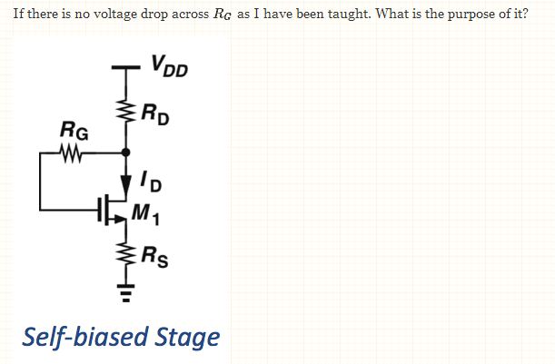
Please help me explain with the highlighted part.
How do you get input impedance of MOSFET, [lATEX] R_{D},[/LATEX] if [LATEX]R_{G} [/LATEX]is zero?
For example, if I hook an voltage source Vin to gate of the transistor, thus:
Input impedance of the circuit at gate, Zin:
[LATEX]Z_{in} = \frac{ V_{in} }{I_{in}} = \frac{ V_{in} }{0} = \propto [/LATEX]
To me, it seems that input impedance of the circuit is always infinity. Please point out what/where I am wrong. Thank you.
 

Attachments

  • Self-biased stage.JPG
    Self-biased stage.JPG
    32.6 KB · Views: 3,239
Simply mark on the digram where is a input terminal for this stage. And try to think what will happen if we have a input signal connect to the input terminal and RG = is zero ohms. And if you look carefully you will see that without RG resistor we short input signal directly to MOSFET drain. So this circuit is no longer a CS amplifier.
 
Thank you, Jony.
I thought about that but I want to apply the definition of input impedance to the circuit.
If RG = 0 then Vin will directly connect to drain of transistor but the input current still has to be zero, IG = 0 not ID .
So the input impedance is infinity not RD .
I agree with you that if RG = 0 input voltage = output voltage and it is no longer a CS amplifier.
My really confusion is in the sentence "We need a resistor to help maintain whatever input impedance is necessary at the gate."
Does RG have something to do with input impedance?
 
If RG = 0 then Vin will directly connect to drain of transistor but the input current still has to be zero, IG = 0 not ID .
So the input impedance isnot RD .
What ?? How can it be infinite anymore ? Please do small-signal analysis for this circuit

self-biased-stage-jpg.80809


And you will find that even if Rg>>0 input impedance is not equal to infinite.

Zin = Vin/Iin = Rg/(1 + Av) --> miller effect

Where Av is a amplifier voltage gain

Av = gm*Rd
 

Attachments

  • Self-biased stage.JPG
    Self-biased stage.JPG
    8.4 KB · Views: 2,212
Thanks Jony. I see that you calculate Zin of small signal, I thought it is for large signal (total signal).
I have just calculated it using small signal model.
Here is the small signal model:
small-signal-model-png.80810

Find V using nodal method:
[LATEX]\frac{V- V_{in} }{ R_{G} } + \frac{V}{ R_{D} } + g_{m} . V_{in} = 0[/LATEX]
Input current Iin:
[LATEX]I_{in} = \frac{ V- V_{in} }{ R_{G} } = - \frac{1 + g_{m}. R_{D} }{ R_{D}+ R_{G} } . V_{in} [/LATEX]
Input impedance Zin:
[LATEX]Z_{in} = \frac{ V_{in} }{ I_{in} } = - \frac{ R_{D}+ R_{G}}{1 + g_{m}. R_{D}} [/LATEX]
I like your method using Miller effect but is there a mistake in numerator? In my calculation, numerator is Rg + Rd.
 

Attachments

  • small signal model.PNG
    small signal model.PNG
    13.2 KB · Views: 1,876
Last edited:
Your equation for Zin is correct. My equation using a Miller effect gives only an approximate value.
 
Thanks, now I see the roles of the resistor.
As in the formula, Zin is proportional to RG. I think we want Zin as large as possible, if so we can choose RG very large. Is the a limited range for RG?
 
I think we want Zin as large as possible, if so we can choose RG very large. Is the a limited range for RG?
One of the limitation factor is a input signal resistance. Because if Rs is very close to Rg the voltage gain will drop to Av = Rg/Rs.
 
I spot a error in your equation. Zin is positive not negative.

[LATEX]Z_{in} = \frac{ V_{in} }{ I_{in} } = \frac{ R_{D}+ R_{G}}{1 + g_{m}. R_{D}}[/LATEX]
 
I spot a error in your equation. Zin is positive not negative.

[LATEX]Z_{in} = \frac{ V_{in} }{ I_{in} } = \frac{ R_{D}+ R_{G}}{1 + g_{m}. R_{D}}[/LATEX]

And if Rd<<RG

[LATEX]Z_{in} = \frac{ V_{in} }{ I_{in} } \approx \frac{R_{G}}{1 + g_{m}. R_{D}}[/LATEX]
 
Hi,

Another 'quick' view is that with the drain connected directly to the gate, with the right constraints on the input (if we had one) the circuit then looks like a resistor RD in series with a current source M1 in series with RS. So in any input to the gate now (with the proper constrains in place) sees an impedance equal to simply RD. So Zin=RD.
Of course maintaining the input constraint would probably not be possible. But for inputs close to that requirement the input Z would look nearly equal to RD alone.
The constraint on the input would be that it has to be a voltage nearly equal to the self biased gate voltage when the gate is shorted to the drain. Again, this probably isnt easy to get, but it does show that the impedance is not infinite, no way, but goes very low as RD will normally be much lower than say 1 Megohm.
 
I spot a error in your equation. Zin is positive not negative.
Thanks, I didn't pay attention to the direction of input current, Iin.
And if Rd<<RG

[LATEX]Z_{in} = \frac{ V_{in} }{ I_{in} } \approx \frac{R_{G}}{1 + g_{m}. R_{D}}[/LATEX]
What is the significance of this evaluation? From the formula, it says that the input impedance will be a constant if load resistance, Rd is much smaller than RG.
We want Zin to be a constant, right? If so, the condition for load resistance is Rd << RG is a must.
 
Thank you, MrAl.
Another 'quick' view is that with the drain connected directly to the gate, with the right constraints on the input (if we had one) the circuit then looks like a resistor RD in series with a current source M1 in series with RS. So in any input to the gate now (with the proper constrains in place) sees an impedance equal to simply RD. So Zin=RD.
Yes, I see it. My mistake was to consider Iin = Ig = 0. That is not true.
The current flows into gate is zero but the current flow across RG is not zero.
Of course maintaining the input constraint would probably not be possible. But for inputs close to that requirement the input Z would look nearly equal to RD alone.
I am not sure what you meant by input constraint. Is it input impedance or input voltage?
The constraint on the input would be that it has to be a voltage nearly equal to the self biased gate voltage when the gate is shorted to the drain. Again, this probably isnt easy to get, but it does show that the impedance is not infinite, no way, but goes very low as RD will normally be much lower than say 1 Megohm.
If you mean input impedance, do you mean that input impedance has to be a constant and the only thing we can do is to choose RD as small as possible but not zero?
 
Hi,

I meant that the input voltage would have to be held constant.

But if we just look at it as a variable current source with variable input voltage, then we see that we have the highest end impedance equal to Rd at the output, and the lowest equal to Rs (ideal device) in parallel with Rd. So we have those two extremes at the output, Rd and Rs, where Rd is the highest we can have and Rp equal to Rs in parallel with Rd as the lowest at the output. So the output looks like either Rd or Rp, and the input looks like Rg in series with either one of those. So the input impedance extremes are:
Rg+Rd
and
Rg+Rp

In other words, if the FET output is an open, we have Rg+Rd, and if the FET is a short, we have Rg+Rp as input impedance.

This is a simpler view i think.

So for a wide operating swing we have a wider input impedance swing if Rs<<Rd and a smaller swing if Rs is close to Rd, but if Rg is high then that always dominates the impedance because the added percent change from either Rd or Rp will always be a small percentage of the total resistance.
 
[LATEX]Z_{in} = \frac{ V_{in} }{ I_{in} } \approx \frac{R_{G}}{1 + g_{m}. R_{D}}[/LATEX]

What is the significance of this evaluation? From the formula, it says that the input impedance will be a constant if load resistance, Rd is much smaller than RG.
We want Zin to be a constant, right? If so, the condition for load resistance is Rd << RG is a must.
Hmm, after this simplification the equation looks exactly the same as a "Miller" equation.

[LATEX]Z_{in} = \frac{ V_{in} }{ I_{in} } \approx \frac{R_{G}}{1 + g_{m}. R_{D}}= \frac{R_{G}}{1 + A_{V}}[/LATEX]

So, the larger voltage gain, the smaller Zin is. And small Zin is not a good think. And this is why we don't use this type of a circuit very often.
 
Hi, Jony.
That seems interesting. From your equation, there is a trade-off between input impedance, Zin and voltage gain, Av. Actually, I am stuck in self-bias technique in RF. That circuit is more difficult than this one. I will post it later. Hope you can help.
 
Thank you, MrAl.
Now I get it. You showed me another way to directly calculate input/output impedance of the circuit not based on small/large signal model. I like this method because it is intuitive to see get impedance.
 
Hi,

I meant that the input voltage would have to be held constant.

But if we just look at it as a variable current source with variable input voltage, then we see that we have the highest end impedance equal to Rd at the output, and the lowest equal to Rs (ideal device) in parallel with Rd. So we have those two extremes at the output, Rd and Rs, where Rd is the highest we can have and Rp equal to Rs in parallel with Rd as the lowest at the output. So the output looks like either Rd or Rp, and the input looks like Rg in series with either one of those. So the input impedance extremes are:
Rg+Rd
and
Rg+Rp

In other words, if the FET output is an open, we have Rg+Rd, and if the FET is a short, we have Rg+Rp as input impedance.

I think you are considering the large signal case where the input voltage swing is large enough to take the FET from to cutoff to full on (or nearly so).

At cutoff the FET certainly behaves as though it were open, but at full on bias the FET doesn't behave like a short. In the full on case, gm may become large, but the gate still has an effect on the output current. The FET only behaves like a short if it really is shorted; damaged, with the gate having lost all control.

If we calculate the small signal input impedance and let gm -> infinity, the impedance reaches a limiting value of Rg + Rs||Rd - (Rg*Rd)/(Rs + Rd). This is equal to your Rg +Rp value with a correction term shown in red.

Hi there Electrician,

That's an interesting reply, but i am afraid i do not follow your logic here. Im sure it is just a matter of a few more words to clear this up though.

What i see so far is that in your equation for Zin, we have:
Zin=Rg+(Rs*Rd/(Rs+Rd))-(Rg*Rd)/(Rs+Rd)

and the negative part is the part you had shown (nicely) in red.

Simplifying Zin we get:
Zin=Rs*(Rg+Rd)/(Rs+Rd)

Using values (note a high Rg as typical) of:
Rg=1000000
Rd=1000
Rs=100

We get:
Zin=Rin=91000 Ohms

This is lower than Rg by a factor of at least 10.

Also, if the output can not get all the way to a short wouldnt that just make Rs look larger?

I can guess that you might be saying that the gate can draw current too, but i would prefer if you can clear this up yourself. Thanks :)
 
Hi there Electrician,

That's an interesting reply, but i am afraid i do not follow your logic here. Im sure it is just a matter of a few more words to clear this up though.

What i see so far is that in your equation for Zin, we have:
Zin=Rg+(Rs*Rd/(Rs+Rd))-(Rg*Rd)/(Rs+Rd)

and the negative part is the part you had shown (nicely) in red.

Simplifying Zin we get:
Zin=Rs*(Rg+Rd)/(Rs+Rd)

Yes, this is the correct expression for the input resistance with gm -> infinity.

The full expression for finite gm is Zin = ((gm*Rs+1)*(Rg+Rd))/((Rs+Rd)*gm+1)

Using values (note a high Rg as typical) of:
Rg=1000000
Rd=1000
Rs=100

We get:
Zin=Rin=91000 Ohms

Yes, that's right for gm -> infinity

For several other values of gm we get:

Code:
  gm      Zin
  .001   524333
  .01    166833
  .1     99198
  1.0    91826
  10     91083


This is lower than Rg by a factor of at least 10.

True enough. That's what gm (and the Miller effect) can do for you.
 
Status
Not open for further replies.

Latest threads

New Articles From Microcontroller Tips

Back
Top