Continue to Site

Welcome to our site!

Electro Tech is an online community (with over 170,000 members) who enjoy talking about and building electronic circuits, projects and gadgets. To participate you need to register. Registration is free. Click here to register now.

  • Welcome to our site! Electro Tech is an online community (with over 170,000 members) who enjoy talking about and building electronic circuits, projects and gadgets. To participate you need to register. Registration is free. Click here to register now.

Input impedance of self-biased stage

Status
Not open for further replies.
Hello again,

Yes i agree now. It's almost like an amplifier where the resistor is in the negative feedback path.

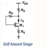
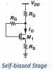
What else is interesting is that with the device biased, with output voltage Vd the input voltage must also be Vd, and with those bias conditions that means the input current is zero (zero through the 1M feedback resistor). I think maybe this was part of what the original question was all about. The input impedance looks infinite, but it's not because as soon as we see some input change we see different operating circumstances and then some real input impedance. Trying to get that condition might be a little hard to do as Rd has to be set with a given Vs to get something that works :)
 
To me, it seems that input impedance of the circuit is always infinity. Please point out what/where I am wrong. Thank you.

There's a difference in the DC resistance and the AC (and RF) resistance.

It may be true that there is no DC voltage across Rg, but if you apply an AC voltage to the gate, an AC current will flow in Rg. In fact, an AC voltage applied to the gate will result in an AC voltage at the drain, and that will lead to a Miller effect reduction of the apparent resistance of Rg. Therefore, the AC (and RF) resistance (impedance) at the gate will not be infinite.

If provision is made to vary the DC bias on the gate without interfering with the application of AC (through a capacitor) to the gate, the input resistance will vary with the gm at the particular bias point.
 
Hi again,

Yes that seems to be the main thing here. With the proper biasing there is no input current, but as soon as we get some AC input going, we see some input current and input current means there must be some non infinite resistance. We can also look at a DC change and see more simply what happens.

anhnha said:
"To me, it seems that input impedance of the circuit is always infinity. Please point out what/where I am wrong. Thank you."

If we had the proper bias, then the output voltage Vd would be equal to the input voltage Vin because there is no voltage across the feedback resistor (which we'll call 1Megohm for now). So if we had 6v on the output we'd have 6v on the input. No current flowing through the 1M, no current flowing into the gate, so it looks like infinite impedance.

Well it is for that one DC bias point. If we connect that constant voltage source i was talking about earlier in this thread, we'd see no current flow if it was equal to the self biased input voltage. That's easy to imagine. But of course we can not use it like that forever because it would not do anything unless it was being used as a reference of some type. So we eventually apply some sort of change to the input, and this is where it gets ever more interesting...

If we again start with 6v on the output and 6v on the input, then increase the input to 6.1v, we'd see the output go lower because it's an inverting amplifier. Now if the voltage gain was equal to 1, we should see the output go down to 5.9v. So with 6.1v on the input and 5.9v on the output, we just caused a 0.2v change from only a 0.1v input change, meaning we're getting 2x the voltage we applied across the resistor instead of just 1x as we normally do when we drive a lone resistor with a voltage source.
So with a lone 1M resistor when we apply 0.1v we get 0.1ua, which equates of course to 1Megohm as 0.1v/0.1ua, but when that resistor is in the feedback path for a 0.1v increase the current through the 1M resistor increases not to 0.1ua but to 0.2ua, and 0.1v/0.2ua equates to 500k ohms now.

So the input impedance went down because of the inverted gain of the 'amplifier'. It is therefore related to the voltage gain of the amplifier as well as the feedback resistance. If the voltage gain was higher like 3 (actually minus 3) we would have seen the output go down to 5.7v so that would have given us 0.4v across the resistor and thus 0.4ua and thus 0.1v/0.4ua equates to 250k ohms.

This trick is actually used in another way too, to INCREASE the input impedance of an amplifier, by using positive feedback instead of negative feedback. Here if we apply a 0.1v input and feed back +0.05v we see only 0.05v across the 1M resistor and that gives us only 0.05ua, and 0.1v/0.05ua makes the input impedance 2 Megohms now.
 
Hi,
I will post my calculation here and please help me check it with some questions.
This is the self-bias circuit:

self-bias-stage-mosfet-png.80877

And here is its small-signal model:

small-signal-model-mosfet-png.80879

And this is my calculation about input impedance of the circuit, Zin:
Calculate V1:

[LATEX]V_{in} = V_{1} + g_{m}. V_{1}. R_{S} = ( g_{m}.R_{S} + 1)V_{1}[/LATEX]
[LATEX]V_{1} = \frac{1}{g_{m}.R_{S} + 1}.V_{in}[/LATEX]
Calculate Vout using nodal method:

[LATEX]\frac{ V_{out} }{ R_{D} } + \frac{g_{m}}{g_{m}.R_{S} + 1}.V_{in} + \frac{V_{out} -V_{in} }{R_{G}} = 0[/LATEX]
[LATEX]V_{in}( \frac{1}{ R_{G }} - \frac{g_{m}}{g_{m}.R_{S} + 1} ) = V_{out} (\frac{1}{ R_{D }} + \frac{1}{ R_{G }} )[/LATEX]
[LATEX]V_{out} = \frac{ R_{D}. R_{G} }{R_{D}+ R_{G} } ( \frac{1}{ R_{G} } - \frac{g_{m}}{g_{m}.R_{S} + 1} ).V_{in}[/LATEX]
[LATEX]I_{in} = \frac{ V_{in}- V_{out} }{ R_{G} } = \frac{1+ g_{m}( R_{D} + R_{S})}{(R_{D} + R_{G})( g_{m}R_{S} + 1)} . V_{in} [/LATEX]
[LATEX]Z_{in} = \frac{ V_{in} }{ I_{in} } = \frac{(R_{D} + R_{G})( g_{m}R_{S} + 1)}{ 1+ g_{m}( R_{D} + R_{S})} [/LATEX]

This value is same as The Electrician, thus, I am sure it is correct.
My confusion is why the method below don't work.
input-impedance-confusion-png.80880


At cutoff the FET certainly behaves as though it were open, but at full on bias the FET doesn't behave like a short. In the full on case, gm may become large, but the gate still has an effect on the output current. The FET only behaves like a short if it really is shorted; damaged, with the gate having lost all control.

I am not quite understand this. The transistor is used as an amplifier, right? This means that it has to be operated in saturation and if so the transistor will never be cutoff, is that right?
If we calculate the small signal input impedance and let gm -> infinity, the impedance reaches a limiting value of Rg + Rs||Rd - (Rg*Rd)/(Rs + Rd). This is equal to your Rg +Rp value with a correction term shown in red.
As gm -> infinity: Is this equal to NMOS is shorted and the gate lost all control?
If gm = infinity then Id also infinity as long as Vg is not zero, and it seems that the gate lost
There's a difference in the DC resistance and the AC (and RF) resistance.

It may be true that there is no DC voltage across Rg, but if you apply an AC voltage to the gate, an AC current will flow in Rg. In fact, an AC voltage applied to the gate will result in an AC voltage at the drain, and that will lead to a Miller effect reduction of the apparent resistance of Rg. Therefore, the AC (and RF) resistance (impedance) at the gate will not be infinite.

If provision is made to vary the DC bias on the gate without interfering with the application of AC (through a capacitor) to the gate, the input resistance will vary with the gm at the particular bias point.
Yes, I see it.
Relating to input impedance, gm and bias point, how can you derive that conclusion? I think you based on the Id-Vgs characteristic. If Vgs increases then gm will increase and as in the input impedance formula, Zin above, gm increases => Zin increases.
But is there an intuitive way to know this without using the formula?
 

Attachments

  • self-bias stage mosfet.PNG
    self-bias stage mosfet.PNG
    50.2 KB · Views: 1,506
  • small signal model mosfet.PNG
    small signal model mosfet.PNG
    11.1 KB · Views: 1,129
  • input impedance confusion.PNG
    input impedance confusion.PNG
    25 KB · Views: 1,057
Hi,

I tried to point out that when you have a single resistor like 1M and a 1v source, you have 1ua. And we can 'calculate' the resistance (impedance) by dividing 1v by 1ua and we get 1v/1ua=1 Megohm. This is with a SINGLE voltage source on ONE side of the resistor, and other side of the resistor going to ground.

But when we have a changing voltage on the OTHER side of the resistor too (not just that one side as before) that means that when we apply that SAME 1v now we might see the OTHER side of the resistor change to some other level, like -1v for example and that's due to the amplification factor.
For this example now we would have 2v across that same 1M resistor and so we'd see 2ua flowing through it (+1v on the left side, -1v on the right side means 2v total across it.). Now when we calculate the input voltage over the current we get 1v/2ua and that equals 500k Ohms now, not 1 Megohm.
The FET causes the change in the output voltage.

That's the most intuitive view i think. Also, the view with the current source being infinite isnt a good view because it is changing.
 
Thank you, MrAl.
Your approach is the most intuitive, imo. I typed the post above before reading your post.
Also, the view with the current source being infinite isnt a good view because it is changing.
Can you explain more, why my calculation using infinite impedance current source is wrong?
Ah, I think it is starting clear to me.:cool:
As you said in this case the current source have its value changes over time and therefore its impedance is not infinite.
 
My confusion is why the method below don't work.
input-impedance-confusion-png.80880

To say that the impedance of a current source is infinity would be true if it were not a controlled, or dependent, current source. But, because the current from the current source depends of Vgs, this means that if Vgs is a small signal AC source, the current from the current source will vary with the instantaneous value of the AC voltage applied to Vgs. This causes the apparent impedance of Rg to vary because of the Miller effect:

https://en.wikipedia.org/wiki/Miller_effect

As it says in that article, "Although the term Miller effect normally refers to capacitance, any impedance connected between the input and another node exhibiting gain can modify the amplifier input impedance via this effect."

I am not quite understand this. The transistor is used as an amplifier, right? This means that it has to be operated in saturation and if so the transistor will never be cutoff, is that right?

The large signal input impedance (as opposed to the small signal input impedance) varies over a cycle of the applied AC signal voltage. If the applied input signal reaches a minimum that nearly cuts off the FET, the input impedance will be a maximum there. Then, at the maximum of the input signal, the FET may be nearly at its maximum gm, and the input impedance will reach a minimum.

MrAl was trying to point out that you could get an approximate idea of the minimum and maximum of that impedance by considering the limiting cases, namely when the FET is cut off, and also when it is full on. When the FET is cut off, it can be replaced by an open circuit. When it is cut off, it can't be replaced by a short; in that case, you have to calculate the input impedance when gm is very large. That would be the limiting case.

As gm -> infinity: Is this equal to NMOS is shorted and the gate lost all control?
If gm = infinity then Id also infinity as long as Vg is not zero, and it seems that the gate lost

Don't consider that gm actually reaches infinity; just consider that it becomes very large. This would be one of the limiting cases.

Yes, I see it.
Relating to input impedance, gm and bias point, how can you derive that conclusion? I think you based on the Id-Vgs characteristic. If Vgs increases then gm will increase and as in the input impedance formula, Zin above, gm increases => Zin increases.
But is there an intuitive way to know this without using the formula?

Actually, as gm increases, Zin decreases, because of the Miller effect. Fully understanding the Miller effect will aid your intuitive understanding.
 
Hi again anh,

Well, the current source change is causing a change in output voltage, and the output voltage change makes the input impedance look different as we figured out because it can cause a change in current through Rg which we dont see when we do NOT allow a change of output voltage. So in other words, with the output voltage constant we'd see a constant input impedance equal to something just above Rg.

It helps more i think to look at the total picture. Sometimes these 'models' are too far removed from reality because they have already taken into account certain presumptions, and if we dont carefully consider those presumptions beforehand things might not look right. So i suggest going back to basics, do the full analysis of the circuit and try to understand it from the point where there are no assumptions. We can start by ignoring Rs for now, and include it later to see it's effects. This simplifies the analysis for what we are looking for and still stays pretty general, but of course we can include that in the final analysis. We're mainly interested in what is happening between the gate and drain right now, so lets look at that in more detail first.

To start, we can write up the equations for Id, Vd, and iRd, then calculate the full Vd. We get:
Vd=(gm*Rd*Rg*Vth+(Rd-gm*Rd*Rg)*Vin+Rg*Vdd)/(Rg+Rd)

where
Vd is the voltage measured from drain to ground,
Rd is the drain resistor,
Rg is the gate to drain resistor,
Vdd is the circuit source power supply voltage,
Vth is the threshold voltage,
gm is the transconductance assumed to be constant,
Vin is the total input voltage measured from gate to ground.
Also, Rs=0 as noted above.

Here we dont assume anything except constant gm, which has been the assumption all along anyway.

One thing to note in particular however is that Vin is measure from gate to ground for this equation. That's not the 'real' Vin though because when we look for the input impedance it is for a circuit that is intended to be used with a previous stage that wants to drive the circuit normally, which means that the input voltage will NOT range from 0 to Max, but will range from approximately Vth to Max. This is important because for one thing there is no reason why we would want the input voltage to go below Vth as that would mean we would be out of the 'linear' range of the circuit.
This important point, however important it is, is made possible with the simple addition of an single input capacitor. The input capacitor allows the previous stage to drive this stage without worrying about the DC levels.

So the first thing we have to do is calculate the bare input, that is, the input without any input voltage source connected to the circuit. To do this we can take the full equation above, replace Vin with Vd (because Vin=Vd at that point), then solve the implicit equation again explicitly for Vd. We get:
Vd=(gm*Rd*Vth+Vdd)/(gm*Rd+1)

Throwing in a couple values:
gm=0.001,
Rd=1000,
Vth=4,
Vdd=10,
(and Rg=1M later),

we get:
Vd=7 volts.

So this is our starting point. We have to make Vin=7 volts just to start. Inserting that into the main equation we find we do get 7v output.

Now we increase Vin to 8 volts, insert that into the equation, and calculate the output Vd is now 6v. Now with 8v on the input and 6v on the output we have 2v across the 1M resistor (Rg) so we have 2ua flowing, and 2ua flowing with our change of 1v means again 1v/2ua=500k Ohms.

So again the whole thing is about the output voltage changing and that makes the input current increase more than it would if there was no output change. The output voltage dropped from 7v to 6v while the input increased from 7v to 8v so we ended up getting more current than we normally would get through Rg. We got more current because the output went DOWN as the input went UP. We'd get less current if the output went up while the input went down and that would make the input impedance higher.

Interestingly, if we increase Vdd to 20 volts, the self bias point is Vd=Vin=12v now, and increasing that to 13v means the output goes down to 11v, and so again we have 2v/1M=2ua and since we only changed the input by 1v again we have 1v/2ua=500k Ohms again. So for the perfectly linear circuit the input impedance is independent from the power supply voltage.

I also agree with Electrician (didnt see his post until after i posted this one) in that understanding the Miller Effect is what this is really all about.

The whole idea here is that an increase in input voltage is causing a much higher current through the input resistor than it would if the resistor was connected to ground. That's because the FET amplifies, but even more basic than the Miller Effect is the fact that the voltage change across the resistor is due to the change of TWO related voltages, not just one voltage change. The second source voltage change makes the impedance presented to the first voltage source look lower when the second source decreases.
We could model this very simply with two related voltage sources where one decreases by 1 volt when the other increases by 1 volt, and we want to know the impedance that the first source 'sees'. It would look lower because there would be more voltage differential than with only one source.
 
Last edited:
Thank you for detailed replies.:D
First, I want to calculate Zin by using Miller effect.
Here is an inverting amplifier with a feedback resistor RG.
self-bias-stage-1-png.80892

According to the article Miller effect in wikipedia, to calculate input impedance of the circuit, we need to know the voltage gain, Av, of the circuit without feedback resistor.
If so it is an CS source with source degeration.
This picture shows the input impedance calculation with Miller effect:

miller-effect-input-impedance-png.80893


To calculate Zin of self-bias stage I need to know voltage gain Av of the aplifier without feedback resistor RG.
This is result from an online lecture:
cs-stage-with-source-degeneration-1-png.80894

Now the input impedance of the self-bias stage will be:


[LATEX]Z_{in} = \frac{Z}{1 + A_{v} } = \frac{ R_{G} }{1 + \frac{ g_{m} R_{D} }{1+ g_{m} R_{s} } } = \frac{ R_{G}( 1 + g_{m} R_{s}) }{1 + g_{m} (R_{S}+R_{D} )} (*)[/LATEX]

This is what I am confused. In my previous post, I have input impedance Zin:

[LATEX] Z_{in} = \frac{ V_{in} }{ I_{in} } = \frac{(R_{D} + R_{G})( g_{m}R_{S} + 1)}{ 1+ g_{m}( R_{D} + R_{S})}[/LATEX] (**)

From (*) and (**), we can see that two results are not the same. In (*) there is no RD.
In my calculation using Miller effect, why RD disapears?
Is there any wrong in my calculation?
 

Attachments

  • Self bias stage 1.PNG
    Self bias stage 1.PNG
    43.5 KB · Views: 1,130
  • Miller effect input impedance.PNG
    Miller effect input impedance.PNG
    30 KB · Views: 2,712
  • CS stage with source degeneration 1.PNG
    CS stage with source degeneration 1.PNG
    73 KB · Views: 2,059
Hi MrAl, thank you for the detailed reply.
I think there is a small mistake here but hope it will not affect much to the analysis.
Here is the circuit:
self-bias-3-png.80895

[LATEX]I_{D} = \frac{1}{2} \mu _{n} c_{ox} \frac{W}{L} ( V_{in}- V_{th} ) ^{2} [/LATEX]

[LATEX] g_{m} = \frac{\partial I_{D} }{\partial V_{in} } = \mu _{n} c_{ox} \frac{W}{L} ( V_{in}- V_{th} ) [/LATEX]

Therefore,

[LATEX]\mu _{n} c_{ox} \frac{W}{L} = \frac{ g_{m}}{V_{in}- V_{th}} [/LATEX]

And:
[LATEX] I_{D} = \frac{1}{2} g_{m} (V_{in}- V_{th} )[/LATEX]

The current flows through Rd:

[LATEX]I_{ R_{d} } = I_{D} + \frac{ V_{d} - V_{in} }{ R_{G} } [/LATEX]

Thus,

[LATEX]V_{d} = V_{dd} - (I_{D} + \frac{ V_{d} - V_{in} }{ R_{G} } ) R_{D} [/LATEX]

Or:

[LATEX]V_{d} = \frac{ \frac{1}{2} g_{m} R_{D} R_{G} V_{th} + ( R_{D} -\frac{1}{2} g_{m} R_{D} R_{G} ) V_{in} + V_{dd} R_{G} }{ R_{D} + R_{G} } [/LATEX]

Here we dont assume anything except constant gm, which has been the assumption all along anyway.

One thing to note in particular however is that Vin is measure from gate to ground for this equation. That's not the 'real' Vin though because when we look for the input impedance it is for a circuit that is intended to be used with a previous stage that wants to drive the circuit normally, which means that the input voltage will NOT range from 0 to Max, but will range from approximately Vth to Max. This is important because for one thing there is no reason why we would want the input voltage to go below Vth as that would mean we would be out of the 'linear' range of the circuit.
This important point, however important it is, is made possible with the simple addition of an single input capacitor. The input capacitor allows the previous stage to drive this stage without worrying about the DC levels.

The capacitor here, I think, you meant coupling capacitor? If we use it then we can bias the circuit to allow it operate in saturation region or at least make it on, without worrying about input DC level.

So this is our starting point. We have to make Vin=7 volts just to start. Inserting that into the main equation we find we do get 7v output.

Now we increase Vin to 8 volts, insert that into the equation, and calculate the output Vd is now 6v. Now with 8v on the input and 6v on the output we have 2v across the 1M resistor (Rg) so we have 2ua flowing, and 2ua flowing with our change of 1v means again 1v/2ua=500k Ohms.

So again the whole thing is about the output voltage changing and that makes the input current increase more than it would if there was no output change. The output voltage dropped from 7v to 6v while the input increased from 7v to 8v so we ended up getting more current than we normally would get through Rg. We got more current because the output went DOWN as the input went UP. We'd get less current if the output went up while the input went down and that would make the input impedance higher.

Thanks, that makes sense. Sorry, because I have made you state this many times.:sorry:

Interestingly, if we increase Vdd to 20 volts, the self bias point is Vd=Vin=12v now, and increasing that to 13v means the output goes down to 11v, and so again we have 2v/1M=2ua and since we only changed the input by 1v again we have 1v/2ua=500k Ohms again. So for the perfectly linear circuit the input impedance is independent from the power supply voltage.
Yes, interesting, also I have just checked Zin in my calculation. Apparently, it is not dependent on voltage supply.
The whole idea here is that an increase in input voltage is causing a much higher current through the input resistor than it would if the resistor was connected to ground. That's because the FET amplifies, but even more basic than the Miller Effect is the fact that the voltage change across the resistor is due to the change of TWO related voltages, not just one voltage change. The second source voltage change makes the impedance presented to the first voltage source look lower when the second source decreases.
We could model this very simply with two related voltage sources where one decreases by 1 volt when the other increases by 1 volt, and we want to know the impedance that the first source 'sees'. It would look lower because there would be more voltage differential than with only one source.
Yeah, I understand now. Because the voltage at two ends of the resistor change oppositely, the voltage across it will increase 2X and thus, current also increase 2x.
If Vin increase n volts and the circuit has voltage gain = 1 => Vout will decrease n volts.
The voltage across the resistor will be 2n volts. Current will be 2n/ Rg.
Input impedance, Zin = n/ (2n/Rg) = Rg/2.
 

Attachments

  • self-bias 3.PNG
    self-bias 3.PNG
    19.9 KB · Views: 1,006
Thank you for detailed replies.:D
First, I want to calculate Zin by using Miller effect.
Here is an inverting amplifier with a feedback resistor RG.
self-bias-stage-1-png.80892

According to the article Miller effect in wikipedia, to calculate input impedance of the circuit, we need to know the voltage gain, Av, of the circuit without feedback resistor.
If so it is an CS source with source degeration.
This picture shows the input impedance calculation with Miller effect:

miller-effect-input-impedance-png.80893

To calculate Zin of self-bias stage I need to know voltage gain Av of the aplifier without feedback resistor RG.

You can't use the formula in yellow because it assumes that the amplifier has zero output impedance. You can't use the gain of your FET circuit calculated without Rg in place because your amplifier does not have zero output impedance; the gain of your amplifier is affected by Rg unlike the "ideal" one in the discussion of Miller effect.

The correct expression is:

[LATEX] Z_{in} = \frac{ V_{in} }{ I_{in} } = \frac{(R_{D} + R_{G})( g_{m}R_{S} + 1)}{ 1+ g_{m}( R_{D} + R_{S})}[/LATEX]
 
Hi MrAl, thank you for the detailed reply.
I think there is a small mistake here but hope it will not affect much to the analysis.
Here is the circuit:
self-bias-3-png.80895

[LATEX]I_{D} = \frac{1}{2} \mu _{n} c_{ox} \frac{W}{L} ( V_{in}- V_{th} ) ^{2} [/LATEX]

[LATEX] g_{m} = \frac{\partial I_{D} }{\partial V_{in} } = \mu _{n} c_{ox} \frac{W}{L} ( V_{in}- V_{th} ) [/LATEX]

Therefore,

[LATEX]\mu _{n} c_{ox} \frac{W}{L} = \frac{ g_{m}}{V_{in}- V_{th}} [/LATEX]

And:
[LATEX] I_{D} = \frac{1}{2} g_{m} (V_{in}- V_{th} )[/LATEX]

The current flows through Rd:

[LATEX]I_{ R_{d} } = I_{D} + \frac{ V_{d} - V_{in} }{ R_{G} } [/LATEX]

Thus,

[LATEX]V_{d} = V_{dd} - (I_{D} + \frac{ V_{d} - V_{in} }{ R_{G} } ) R_{D} [/LATEX]

Or:

[LATEX]V_{d} = \frac{ \frac{1}{2} g_{m} R_{D} R_{G} V_{th} + ( R_{D} -\frac{1}{2} g_{m} R_{D} R_{G} ) V_{in} + V_{dd} R_{G} }{ R_{D} + R_{G} } [/LATEX]


The capacitor here, I think, you meant coupling capacitor? If we use it then we can bias the circuit to allow it operate in saturation region or at least make it on, without worrying about input DC level.


Thanks, that makes sense. Sorry, because I have made you state this many times.:sorry:


Yes, interesting, also I have just checked Zin in my calculation. Apparently, it is not dependent on voltage supply.

Yeah, I understand now. Because the voltage at two ends of the resistor change oppositely, the voltage across it will increase 2X and thus, current also increase 2x.
If Vin increase n volts and the circuit has voltage gain = 1 => Vout will decrease n volts.
The voltage across the resistor will be 2n volts. Current will be 2n/ Rg.
Input impedance, Zin = n/ (2n/Rg) = Rg/2.

Hi again,

Ok if you want to use 1/2 gm instead of just gm that's fine with me. I just wanted to make the other points more clear but i guess it doesnt matter that much overall. So for your result you must 'pretend' that gm is 0.002 instead of 0.001 in my equation for Vd with Rs=0. See we have been assuming a piecewise linear voltage dependent current source for Id, so i stayed with that.

Yes coupling cap.

The input impedance derived from my equation comes out to:
Zin=(Rg+Rd)/(gm*Rd+1)

and:
Vd=(gm*Rd*Rg*Vth+(gm*Rd*Rs-gm*Rd*Rg+Rd)*Vin+(gm*Rg*Rs+Rg)*Vdd)/((gm*Rg+gm*Rd)*Rs+Rg+Rd)

It is interesting that for a zero input change we seem to have infinite input impedance, but that's not the case.

So i used:
Id=gm*(Vin-Vth)

for my approximation to Id, but we can use 1/2 gm if you feel more comfortable with that.

You should check to see that you can get that Zin above. Once you can get that you can do it with Rs too and see what happens.

Note that to get from the equation for Vd to the equation for Vd_self bias you only need to replace Vin with Vd and then solve that again for Vd. This gives you the self bias point input and output voltage Vd1.

Then subtract Vd equation above from Vin and divide by Rg (that's Iin), then set Vin equal to Vd1+dv in that result to get Iin(dv), then do the division dv/Iin(dv) and that's the input impedance. So there we use the partials to get the result.

If you dont mind stating your equations in their entirety we can go over them one by one and see which one doesnt work or whatever. Sorry if this is a repeat, but it's nice to see them all in one shot.

BTW i get the same result as Electrician for the input impedance with Rs included:
Zin=(Rg+Rd)*(gm*Rs+1)/(gm*Rs+gm*Rd+1)

It's also a little interesting that the gain of Zin with Rs isnt affected too much with the values i had been using, but for other values like larger gm it starts to have more of an effect. For example, around 200 Ohms per Ohm as is, but for gm ten times larger it's round 825 Ohms per Ohm. We dont see *this* effect with a constant current source either.
 
Last edited:
Status
Not open for further replies.

New Articles From Microcontroller Tips

Back
Top