Electro Tech is an online community (with over 170,000 members) who enjoy talking about and building electronic circuits, projects and gadgets. To participate you need to register. Registration is free. Click here to register now.
Welcome to our site! Electro Tech is an online community (with over 170,000 members) who enjoy talking about and building electronic circuits, projects and gadgets. To participate you need to register. Registration is free. Click here to register now.
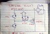
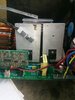
The upper and lower FETs must have totally separate gate drive signals, as the gates can only stand somewhere around 20V maximum and you have a DC supply of around 320V.
There are specially designed "high side" driver ICs to control the upper FETs in such H-Bridge circuits; remember that the upper gate drive is relative to the source of each device - which is changing in voltage over a wide range as the various devices switch on and off.
The output from an H-Bridge is taken between the two centre junctions, where you have the heavy link. If either diagonal pair of transistors switched on, they would short the supply.
If you are trying to trace the circuit of a machine, either the transformer is connected between the centre junctions, or both upper devices are driven simultaneously and both lower devices are driven simultaneously.
eg. A half-bridge with parallelled power devices, rather than the crossed gate connections.
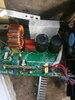
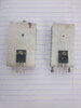
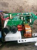
The device came with two 50t65 which is 100a + 100a =200a, while I couldn't find it, that is why I wanted to use 60N60 which is 60a * 4 =240a.
With the look of things which one is preferable among the diagram
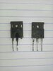
The 50T65 is rated 50A RMS, 650V maximum.
The 60N60 has a higher current rating at 60A, with a 600V maximum.
They are both rated for 15V gate-emitter, so the 60N60 could be a 1:1 replacement with better ratings, as long as the switching frequency is not too high; it's a slightly slower device than the 50T65.
Paralleling more devices than in the original setup is not a good idea as they have very high gate capacitance and doubling that with two in tandem would further slow the switching and increase device heating and power losses.
But I needed 200a, though the 50t65 maximum power dissipation is 100A, since I couldn't find it I intended to use 60N60 which 60a,
That was why I wanted to pair it
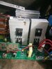
"Maximum" or "peak" current are for short duration pulses, often how much they can take for eg. 10mS.
They are the threshold-of-destruction figures, not operational values.
See the headline data in the datasheet here: 650V 50a.
FGH50T65UPD Field Stop Trench IGBT Components datasheet pdf data sheet FREE from Datasheet4U.com Datasheet (data sheet) search for integrated circuits (ic), semiconductors and other electronic components such as resistors, capacitors, transistors and diodes.
datasheet4u.com
It's also part the device name; 50A & 65(0) volts, as with the 60N60: 60A & 60(0) volts.
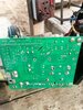
They are both TO-247 packages and have the same pinout, so the 60N60 is a direct drop-in replacement.
If you wanted an even higher rated one, you could possible use these; again physically interchangeable, but somewhat higher gate capacitance which may slow the switching.
They are both TO-247 packages and have the same pinout, so the 60N60 is a direct drop-in replacement.
If you wanted an even higher rated one, you could possible use these; again physically interchangeable, but somewhat higher gate capacitance which may slow the switching.
They are both TO-247 packages and have the same pinout, so the 60N60 is a direct drop-in replacement.
If you wanted an even higher rated one, you could possible use these; again physically interchangeable, but somewhat higher gate capacitance which may slow the switching.
This site uses cookies to help personalise content, tailor your experience and to keep you logged in if you register.
By continuing to use this site, you are consenting to our use of cookies.