Electro Tech is an online community (with over 170,000 members) who enjoy talking about and building electronic circuits, projects and gadgets. To participate you need to register. Registration is free. Click here to register now.
Welcome to our site! Electro Tech is an online community (with over 170,000 members) who enjoy talking about and building electronic circuits, projects and gadgets. To participate you need to register. Registration is free. Click here to register now.
Well the thing is BJT's have the lowest Vsat and they also dont have a intrisnic diode. Only limitation with them are that they are current-driven and are slow
Yeah, no intrinsic diode appeals to me and I've considered BJT's / IGBT's. The only problem is I have a need for the series combination to look like less than 1 Ohm at high currents (5-10A) I also will have some 0.1 Ohm current sense resistor in series so my gut tells me I need some kind of a power fet that I can turn on real hard to get down below 0.3 Ohms or so at high current. Admittedly, I havnt looked into the details of whether or not I can find an IGBT to do that but I'm going off of the assumption that their conduction mechanism is Bipolar technology and should have similar Vsat characteristics. I could be wrong though! Plus FETS might be lower cost for a 10A device. Thanks for the suggestion.
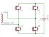
I havnt talked much about my specific application since the thread started as a simple question but I am working on designing a programmable precision power resistor using mosfets. The whole circuit will be floating and the resistance will be symmetrical from either side. These series mosfets will be acting like the "resistance" They will be capable of withstanding 100's of volts, upto 10A and dissipate up to 50W.
What I am concerned about is leakage through the body diodes at high programming resistances. This leakage is hard to compensate for and is very dependent on temperature (which, by the way, could be a broad range)
Anyways, I was hoping to get rid of the diode altogether.
The body diode is not always such a bad thing. It depends on your app.
For example. if you want to build a cool and efficient FWB rectifier, you would orient the MOSFETs so the body diodes act just like a normal diode FWB when the gate drivers are turned off. So turning on the gate driver just brings the vds down from 0.7v to millivolts but otherwise it works either way.
This is true. If you use PWM controllers for the gate drives, you can get some with "dead time" control to avoid shoot through.
Another way to alleviate the issue is to put some series inductance with the FETS to at least keep the currents from rising too high before the complimentary FET turns off.
Yes, that problem exists with any implementation regardless of the number of transistors or whether they're MOSFET or bipolar.
The problem is lessened due to the presence of the body diodes in a functional FWB implementation- the diodes will catch the turn-off spikes and continue to function as a rectifier, so prematurely turning off one transistor to make a clearance before turning on the other leg will not have very negative consequences.
From what I can tell, a hand-cranked generator will not be a really high frequency job so generous latentcies between turning off one and turning on another would not constitute a whole lot of the waveform. Switching losses from charging and discharging gates are also not very big.
I am not sure of the exact application here, but if it is just an efficient FWB, you could use a FET bridge module. They can be had with steering logic to prevent shoot through, and are a nice simple package to use.
There was a company called Gentron that made Powertherm modules that look like a typical solid state relay, they had exactly what you need. There were large screw terminals for the power connections, and small terminals for the control signals. A quick google didn't turn up the company, but they may have changed names or were bought up.
A few years ago we had used their modules in a high current supply ( 0-28 VDC, 50 Amps ) that had regulation controlled by one of these modules.
(edit) requirement were posted during the writing of my post
Yes, that problem exists with any implementation regardless of the number of transistors or whether they're MOSFET or bipolar.
The problem is lessened due to the presence of the body diodes in a functional FWB implementation- the diodes will catch the turn-off spikes and continue to function as a rectifier, so prematurely turning off one transistor to make a clearance before turning on the other leg will not have very negative consequences.
From what I can tell, a hand-cranked generator will not be a really high frequency job so generous latentcies between turning off one and turning on another would not constitute a whole lot of the waveform. Switching losses from charging and discharging gates are also not very big.
They were not the "shootthroughs" I was talking abt.
I really should write a short motor-drive tutorial for this site.
How you have the FET's or switches arranged you must be providing the complemetory version of PWM to the upper and lower devices in a leg.
There is a finite switching time involved. Thus if they are fed the signals at the same time, one will be turning off as the other is turning on, there will be a short across the supply - be it while the switches are in the active region, but still a short.
Some form of interlock is needed to ensure that this does not occur. Such switching shoot-throughs can cuase some serious problems. I overlooked it on a gateboard of mine a shile back. It had a P-N totem pole output (to provide +15 and -15 to the gate of an IGBT), now it was supplied with a 6W TRACO DCC converter, now the board was getting close to that and it was not driving the IGBT hard enough.
Eventually tracked it down to a very short (200ns) period during switching when the top and bottom FET were in a conduction state. I delayed the switching time (via diodes,caps and resistors) and the power of the board went from just abt 6W to 3W.
this kind of thing is a real problem and I have seen it overlooked in cheap drives (for the sake of a couple of diodes,caps and resistors) and their life is not that long.
Right, you can't tie the complimentary gates together, that's why I did not connect them in the schematic.
You could have a circuit that turns on one NMOS and one PMOS whenever the input voltage >0.1v and another that turns on the other pair when input voltage <0.1v. So no overlap as long as the turn-off time is not too long for the highest frequency used.
Or you could just use an op amp on each Vds, so when the Vds exceeds 0.1v it increases the gate voltage. Note you have to establish a nonzero value as a threshold because of the offset error of the amp and again to allow for some spacing for turn-off time. There may also be some issue operating this close to the rails for some amps.
What problem did you see?
The body diode may be slow. Some transistors are built with faster ones. From what you said about hand cranking it sounded like the AC signal would be of a low freq, though perhaps with enough gearing that could change. Perhaps paralleling it with a faster diode might improve its characteristics, I'm not sure. If you paralleled it with a schottky the body diode is sure never to forward bias. But really the diode should never forward bias in normal operation if you drive the gate before the signal reaches 0.7v, so I don't know what your problem would be. Please elaborate on what you have seen.
Note your original schematic runs those transistors the exact same way. The only difference is it adds a blocking transistor to block current to a transistor which is already off. It may allow a different scheme for preventing shoot-though current, but will require additional driving circuitry as well as additional transistors. That not only means extra parts but more current to run them.
What you may find is, depending on how frequently it switches, the current expended switching a gate becomes siginificant. It varies quite a bit by which MOSFET you select too. Also look at what rds is at the gate voltage you intend to use. Higher gate voltage means you will be expending more power every cycle on the gate charge. But MOSFETs usually spec the rds(min) at a high gate voltage, using 3v, 5v or whatever for the gate means substantially higher rds. "Logic level" MOSFETs turn on quite well with 5v.
Congratulations in coming up with the world's most convoluted example of a FWB.
Now the original point was to make a FWB without the 1.4v diode dropout. This circuit leaves the diode drops in place, but adds transistors for no reason whatsoever. Nor do I understand how it's going to perform a blocking function, the diode parallel diode will conduct one way, the MOSFET will conduct if going the other way, so I don't see how it functions as a FWB anymore.
QUOTE
ok fiar enough, however for anyone else running inot intrisic diode problems ill post this
The intrinsic diode present in MOSFET packages arew normally crap when used as free-wheel diodes in H-bridge arrangement, thus this method blocks the intrisic diode allowing you to use a better match (since intrisic diode characterists are nothing like their parent MOSFET - for starters they are more like Zeners)
You want the most efficient FWB but insist on using MOSFET's !!!
BJT have the lowest forward drop and conduction losses, hence if you look at the POWER-electronics table BJT's are still used when fully-controlled is need and very high current are needed to be controlled - their failing is their slow switching (still in the KHz range) and that to switch 1000A you need to at least source and sink 100A or there abouts
This site uses cookies to help personalise content, tailor your experience and to keep you logged in if you register.
By continuing to use this site, you are consenting to our use of cookies.