Electro Tech is an online community (with over 170,000 members) who enjoy talking about and building electronic circuits, projects and gadgets. To participate you need to register. Registration is free. Click here to register now.
Welcome to our site! Electro Tech is an online community (with over 170,000 members) who enjoy talking about and building electronic circuits, projects and gadgets. To participate you need to register. Registration is free. Click here to register now.
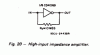
They are sometimes used to attain rail-rail output from a non-rail-rail o/p opamp by placing an even number of series gates at the opamp output (still within the -ve feedback loop).
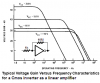
RCA invented Cmos logic ICs a long time ago. They show the analog voltage gain with a 10M feedback resistor and a 1k input resistor at various supply voltages.
I have attached their graph.
The voltage gain is about 30dB (32 times) with a 12V supply. The first first amplifier in your schematic has no input and no input resistor but it has a piezo sounder across the feedback resistor and I do not know why.
The second amplifier has a 4.7M feedback resistor and the output resistance of the first amplifier is about 500 ohms so its voltage gain is about 32 times.
The third, fourth and fifth amplifiers are not biased properly so they will work poorly.
The fifth inverter is simply a logic inverter.
Any CMOS input that is AC coupled without bias (preferably from another device or its own output) is asking for trouble. You can end up drawing too much current as the input is indeterminate as no current flows through a capacitor when stable and thus the input voltage could be anything it wants. I could easily oscillate.
Even if the amps were biased correctly which they are not (see my previous posts) the gain is so high you are relying on frequency variations as there will be no amplitude component (the amps are all saturated). Therefore anything from a mouse croak to a door slamming will trigger it.
R3? What's the point other than an attempt to make a comparator. With so much gain, it will be pointless.
You could achieve the same with a dual opamp. One for the gain, the other as a proper comparator.
The purpose of resistor R3 is to hold the input high on IC1f, in the absence of a clap signal.
So the output of IC1f is held low and it will not charge C8/R4 via the D3 diode.
When a clap signal is input to IC1f its output will switch high and low at the signal frequency of the piezo sounder. The high going pulses will charge up C8 and eventually produce a postive going pulse at the CLK input of the 4017, this will set Q1 high on the 4017.
When the clap period signal stops at IC1f output, C8 will slowly discharge via R4, preparing the 4017 CLK input for the next clap positive going pulse.
So IC1f is not a comparator.
I think the circuit is very poorly designed and will not give the performance that the OP is expecting.
The purpose of resistor R3 is to hold the input high on IC1f, in the absence of a clap signal.
So the output of IC1f is held low and it will not charge C8/R4 via the D3 diode..
Surely by the time any signal gets to R3 it will already be rail to rail signal (mainly audio background noise that has saturated the previous stages) .
last time i check circuit have mic non invert amp filter digital stable latching t
going in breadboard ok it work ok but on pcb it not responds
here is the schematic
i check it on PCB long time but i don't understand the problem
so i search for another one that is the subject here
i am confused about that
This site uses cookies to help personalise content, tailor your experience and to keep you logged in if you register.
By continuing to use this site, you are consenting to our use of cookies.