Continue to Site

Welcome to our site!

Electro Tech is an online community (with over 170,000 members) who enjoy talking about and building electronic circuits, projects and gadgets. To participate you need to register. Registration is free. Click here to register now.

  • Welcome to our site! Electro Tech is an online community (with over 170,000 members) who enjoy talking about and building electronic circuits, projects and gadgets. To participate you need to register. Registration is free. Click here to register now.

Battery switch using MOSFETS

Status
Not open for further replies.

xeno

New Member
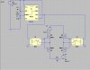
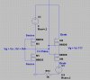
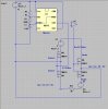
I want to connect two batteries in parallel using MOSFETs.
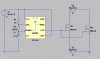
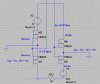
The condition is that the batteries must not be connected at all when the MOSFETs are open. I am aware of that relays can be used to, but out of curiosity i wonder if there is a clever way to do this with MOSFETs (switching speed will be higher than what relays can do also)

The thing that boggles my mind is that the source of the MOSFET can not be grounded and there is no single-directional current flow, so i am having difficulties creating the conditions to operate the MOSFETs as switches (Gate to source voltage difference)

Any ideas would be greatly appreciated
 

Attachments

  • Parallel.jpg
    Parallel.jpg
    61.1 KB · Views: 697
Yeah, it's a really common problem- switching NMOS on the high-side. You need a floating supply of some kind. The cheapest way is a high-gate drive circuit that uses a bootstrap capacitor. It will not allow for 100% duty cycle though because you need to turn the MOSFET off for a short-time (and have it's source go to ground somehow...generally through a complimentary low-side NMOS that is found in such applications to recharge the bootstrap capacitor before you can float it up to the high-side MOSFET source again), unless you add in a separate floating charge pump. But due to the way it works, it can only turn on and activate after the high-side FET is already on, so you still need the bootstrap cap and associated circuitry to get everything started.

If you are not using PWM and just switching on and off, linear technology has some circuits designed to allow high-side NMOSs to substitute PMOS...I am under the impression that they do have the circuitry built-in to allow 100% duty cycle. They even have completely integrated charge pumps so no external caps are needed.

-High Gate Drive Current For PWM
-Higher voltages available...much higher...gate drive supplies tend to be 10-20V and can work with FETs working with voltages source of of 100-1200V. I found some ones that work with logic level voltages for the gate drive supply...they seem very rare because I guess most switching power applications use 10-20V gate MOSFETs rather than use logic level. Of course, these logic-level tolerate less floating source voltage more in line with the drivers in the next section.
-External components required (bootstrap capacitor and diode, though diode is sometimes integrated with more convenience but less performance)
-No Integrated Gate Drive Voltage supply

**broken link removed**
Linear Technology - LTC4440-5 - High Speed, High Voltage, High Side Gate Driver LTC4440-5
Linear Technology - LTC4440 - High Speed, High Voltage High Side Gate Driver LTC4440 LTC4440EMS8E#TR LTC4440EMS8E-5 LTC4440ES6-5#TRPBF LTC4440ES6#TRPBF LTC4440EMS8E#PBF LTC4440EMS8E-5#TR LTC4440ES6-5 LTC4440EMS8E LTC4440ES6-5#TRM LTC4440EMS8E-5#TRPBF

Not PWM Capable (Low drive current)... made to allow NMOS replacement of PMOS load switches
-Lower Voltages (logic level voltage gate drive seems quite common)...and they can often handle FET switching voltages of 36V~100V or so.)
-Fully Integrated charge pumps (internal caps too!) to generate sufficient gate drive voltage for low voltage systems
-Allows 100% duty cycle (as far as I can tell because a <100% load switch is a bit useless in most cases).

Linear Technology - LTC1154 - High-Side Micropower MOSFET Driver LTC1154 LTC1154CS8#TR LTC1154CS8 LTC1154CS8#TRPBF LTC1154HS8#TRPBF LTC1154CN8 LTC1154CS8#PBF LTC1154CN8#PBF LTC1154HS8#PBF
Linear Technology - LTC1163 - Triple 1.8V to 6V High-Side MOSFET Drivers LTC1163 LTC1163CS8#PBF LTC1163CN8 LTC1163CS8#TRPBF LTC1163CS8 LTC1163CN8#PBF LTC1163CS8#TR
Linear Technology - LT1161 - Quad Protected High-Side MOSFET Driver LT1161 LT1161ISW#PBF LT1161IN LT1161IN#PBF LT1161CSW LT1161CN#PBF LT1161CSW#TRPBF LT1161CSW#TR LT1161ISW#TRPBF LT1161CN LT1161ISW LT1161CSW#PBF LT1161ISW#TR
Linear Technology - LTC1165 - Triple 1.8V to 6V High-Side MOSFET Drivers LTC1165 LTC1165CS8#TR LTC1165CN8#PBF LTC1165CS8#TRPBF LTC1165CS8 LTC1165CS8#PBF LTC1165CN8

App Note for 100% duty cycle charge pump (required if you need a 100% duty cycle higher voltage load switch or 100% duty cycle capable PWM):
https://www.electro-tech-online.com/custompdfs/2009/03/an-978.pdf
Page 17

Of course, if you need a high-side driver combined with a low-side driver, you can also find them together in the same IC, for 1, 2, and 3 phases. None are all very far from where the above items are...just hunt around the website starting with the product category they are originally in...an example:
**broken link removed**
 
Last edited:
@ dknguyen: Thanks for the detailed answer, i will read up on the matter as this presents a higher complexity than i anticipated for the application. Thank you for the links also, i will go through them to experiment with components.
 
BTW, you know the MOSFETs only block current in one direction right? I haven't gone through it carefully because I'm lazy and I'm not sure what you want the circuit to do, but I have suspicions about the circuit and the ability of the MOSFETs to do what you want them to do...there's basically a diode in anti-parallel with each NMOS.
 
Last edited:
Hi,


Just a quick note...


Usually when you want to get a MOSFET to turn on with battery equipment
you run the gate to the opposite polarity of where the source is connected.
This keeps a decent gate voltage present for turning it on.
This might require an N channel or P channel depending on your circuit.
 
Hi,
Just a quick note...

Usually when you want to get a MOSFET to turn on with battery equipment
you run the gate to the opposite polarity of where the source is connected.
This keeps a decent gate voltage present for turning it on.
This might require an N channel or P channel depending on your circuit.

Of course, you gotta be careful if your voltage supply is a higher than the tolerable gate voltage. This tends to go unnoticed more with a PMOS that is kept off with a pull-up resistor and is conveniently pulled down to ground to turn it on.
 
Last edited:
Thanks for your detailed ideas!

BTW, you know the MOSFETs only block current in one direction right?

Then would i maybe have to use 2 MOSFETS connected source to source to resolve the blocking into both directions?

I need the batteries to equalize their charges when switched into a parallel constellation to then be used to drive a load.

I will have the signal maybe 10% of the duty cycle high and the rest low (the schematic was simplified), so i assume that this fullfills the case of a < 100% duty cycle in the way you referred to it, right ?
 
Last edited:
Then would i maybe have to use 2 MOSFETS connected source to source to resolve the blocking into both directions?

I need the batteries to equalize their charges when switched into a parallel constellation to then be used to drive a load.

If the voltage was always + on the drain and - on the source for an NMOS you'd be fine with just one since that's the direction of current it will block. But if ever a situtation arises in the circuit where it was - on the drain and + on the source, then you would need back to back MOSFETs. The source drain and +/- stuff is reversed for a PMOS. Back to back MOSFETs are one way of making a solid-state relay (since electro-mechanical relays don't care about polarity at all). You then have the tricky bit of how to drive the gates with respect to the source voltage.

I will have the signal maybe 10% of the duty cycle high and the rest low (the schematic was simplified), so i assume that this fullfills the case of a < 100% duty cycle in the way you referred to it, right ?
It depends on the frequency too. Obviously something like on for 36.5 days and off for the remainding 328.5 days in a the period of a year can't be viewed as 10% duty cycle from speed at which electronic circuits work at. THe bootstrap capacitor has to be able to provide all the necessary charge to switch the MOSFET and keep it on between recharging opportunities (in most circuits whenever the FET is switched off, there is a change to recharge). So it's really a matter of duty cycle and frequency.
 
Last edited:
Back to back

Thanks for hinting me to the back to back configuration.
I still have problems getting the right side to switch (attached schematic) since
the gate signal is too equal to source.
Maybe if i invert the gate voltage for the right side switch, then i could
use PMOS units.

So how could i correctly invert the gate voltage?
Like this? : https://www.electro-tech-online.com/threads/help-inverting-signal-for-fets.42257/

Ah and the frequency is around 100 Hz ( so not 1 year hehe)

Too bad that the battery parallel switching cant be properly simulated.
 

Attachments

  • Parallel2.jpg
    Parallel2.jpg
    88.8 KB · Views: 402
Last edited:
Look at one pair of back-to-back MOSFETs. If you look carefully enough you might notice that for the top FET to turn on you need a gate low gate to be a low voltage to produce the needed gate-source voltage difference to turn the FET on. For the bottom FET you need a high voltage. THat means to turn on you need the same node to be two different voltages simultaneously!

There are two problems:

1. The gate voltage being applied to the FETs means different things between the two FETs because their reference for the gate-source voltage (the source pin) is not the same between the two. Try flipping your FETs around and connecting them source-to-source instead...that way the gate-source voltage on both FETs will share the same reference (the source node) and so you can share the gate voltage. his way, the same gate voltage will cause the same gate-source voltage on both FETs so they will both either turn off or on (rather than one turning off and the other turning on)...under one very important condition (see #2).

2. WIth #1 taken cared of, it is also logical that the gate voltage you are applying also has to be sharing the same reference as the gate-source voltages of the FETs (ie. you need the same type of floating gate supply like the bootstrap circuit). With this last point, the same voltage applied to the two gates will produce the same gate-source voltage across both MOSFETs causing them to behave the same (both on or both off).

A graphical explanation of these two points are shown here:
**broken link removed**

Of course...you could always just keep your configuration and use two separate floating voltage sources each referenced to each FET's source pin and drive each gate pin separately...but why do double the work and double the parts when you can get away with one? Neat huh?

100Hz is quite slow. THe bootstrap capacitors required to sustain the gate for such a period of time might be too large and expensive. Best to do the other calculations in that app note to estimate the capacitance required. Use good ceramic capacitors that have low leakage since once the FET gate capacitance is charged and the FET is on, it draws very little current. Most of the charge is initially used to charge the gate capacitance to turn the FET on, so using FETs with low gate charge lets you use smaller capacitors or lets you use the excess capacitance of the same capacitor to store the charge required to compensate for the gate's leakage current, allowing you to sustain the FET's on-time for longer. If the charge required to turn on the capacitor or the charge to sustain the on-state for the required period of time is too large (or both), consider the charge pump circuit in my app note in my previous post that will allow you to use a smaller capacitor.

One more thing if you are going to equalize the charges you might want to add a resistor or something to slow down the equalization between the batteries...think about it...connecting 5V battery in parallel with a 4V battery is the same as putting a short-circuit across a 5V-4V battery. Not a good thing.
 
Last edited:
Okay, i modified the circuit to a common source configuration of the MOSFETS.
Now i need to understand the bootstrap concept to integrate it.
Thanks for the help.

I also wonder if an inverting op-amp would be best to invert the gate signal?
I need to create a -9V signal for the PMOS side.
 

Attachments

  • Parallel3.jpg
    Parallel3.jpg
    87 KB · Views: 466
The sources of the MOSFET are floating. THey have to be like that to not ruin operation of the circuit. For example, rIght now, if a FET turned on for whatever reason you would get a short-circuit straight to ground.

Imagine we placed connected an isolated/floating (as in not connected to anything else except the things I'm about to say) voltage source to between gate and source with the negative pin of the voltage source connected to the battery and positive pin connected to the source. If we say made the voltage source 0V (a piece of wire basically) the FETs would stay off right? And if the voltage source was made something like 5V or 10V the FETs would turn on, correct?

Okay, now we can make such an isolated voltage source a few ways...we could use isolated DC-DC converters that use transformers so the input ground does not have to be the output ground...big, bulky, expensive, complex, overkill for this application not to mention there are some "gotchas" regarding FET switching noise travelling backwards into the converter and disrupting it, among other things. We could also use transformers directly with and other methods...

What if we used a battery for the voltage source? Great! But now we basically can't turn it off (or if the battery is dead we can't turn it on). What if we made a completely separate circuit completely powered by the battery and the ground of this circuit would be connected directly to the ground source of the MOSFET. THis circuit would accept inputs and send out a voltage into the gates so we could turn the FETs on and off. All voltage outputs from this circuit would be with respect to the source. So a 10V output from this circuit would be a 10V relative to the source of the FETs. Stick that into the gate and voila! It turns on. This circuit is considered "floating" because it's "reference voltage" isn't fixed- it's not relative to ground. It moves up and down with the FET source voltage.

A bit extravagant right? Again, we have a whole extra power supply (the battery) dedicated to the gate. What can we do? What if we charged up a capacitor to the required gate-source voltage difference needed to turn the FET on (to turn it off we can always just short the gate and source pins producing 0V difference- that's easy.). It turns out, we can. Better yet, we can do it with circuitry that uses the system ground as it's reference. What we basically do use switches to connect the + and - of the capacitor across a ground-referenced power supply and let it charge up. THen we disconnect both capacitor terminals using the switches leaving a 10V charged capacitor that has no pins connected to anything. We use a third switch now to connect the NEGATIVE pin of the capacitor to the SOURCE pin of the FET. Suddenly, the voltage on the postive pin of the capacitor is "Source Pin Voltage relative to ground+10V". If we connect the positive pin to the gate, we suddenly get 10V across the gate-source pins and our FET can turn on.

THis is bootstrapping- the IC uses it's own voltage to lift itself to a higher level sort of like pulling yourself out of quicksand by bending over and pulling yourself out by tugging on your boot's straps. Use an IC (you are looking for a high-side gate driver IC). from the resources I posted. THat's just the concept of how it works. There's a lot of crap inside those ICs to actually pull off this off. Pick an IC that meets your requirements and the datasheet will have the schematic.

BTW, the diode on the ICs are there to only allow charge flow from Vgate_drive_supply into the capacitor but not the other way around. That's because when the capacitor's negative pin gets connected to Vsource the + pin of the capacitor is going to be Vsource+Vgate_drive_supply above ground, which would then cause the capacitor voltage being used to drive the gate to drain back into V_gate_drive supply. THe diode only lets charge flow from Vsupply into the capacitor, and the charge from there can only ever flow into the gate.
 
Last edited:
Interesting!
Well as of now i DO have a separate 12 V battery powering the timing circuit.
So i could use that battery`s negative to ground the source pins of the MOSFETs. Thanks for your explanation of the bootstrapping, i have learned a lot about this with this thread.
Right now i am looking at my circuit and wonder if i really need a capacitor that charges itself higher, because i believe that the voltage differences are sufficient on both switch-sides.
Would there still be a short-circuit if a completely different battery is connected to the source? Maybe the electrons would seek that path in all cases?
In that case a bootstrap IC is the only way to go, i understand.
As it is now:
On the left side i have the negative poles of both batteries at the drain pins and a positive 9V gate signal with a potential difference of 9 Volt.
On the right side i have the positive poles of both batteries at the drain pins and a negative 9V gate signal with a potential difference of -9 Volt.
 

Attachments

  • Parallel4.jpg
    Parallel4.jpg
    75.5 KB · Views: 277
Oh, you could also just use an optoisolator gate driver. It would basically be like making your own solid-state relay. THe optoisolator generates an isolated floating voltage on it's outputs from the LED's energy being sent into it on the input side. It has it's disadvnatages, but is much easier for you than boostrapping in this case.

THe reason I bring this up is because of the peculiarity of your circuit. These boostrap circuits need the source to fall to ground when the FET turn off (unboosting the bootstrap capacitor's voltage) for a certain period of time to provide a path from +V to GND to recharge the bootstrap cap. Your circuit actually has the high-side and low-side turning on at the same time. So when the FETs turn off, the charge path is disconnected...which means regular boostrapping won't work...unless you add a resistor to provide a charge path for the capacitor to ground when the FETs are off since it can't go through the low-side FET like normal. The resistor value can't be too small because there would be overheating and it would defeat the purpose of having a switch there. It can't be too large either or the capacitor would take too long to recharge.
 
Last edited:
I guess i will try the opto-isolator then. In any case i would have to purchase an additional component for the MOSFETs to realize this.
A 4N27 should do the job for IRF640/840 i guess.
This looks promising now, thanks again for your precious time! :)
 
I just noticed, you can't tie the PMOS sources and the NMOS sources like that. THe two nodes are not sharing the same reference and you are trying to share the same gate drive voltage. You will need a drive circuit like an opto-driver for each.

Also, you don't need PMOS. It makes no difference in this case and NMOS works better.
 
Last edited:
So i have come up with this now.
Not sure about the output connections on the 4n28s though.

EDIT: forgot about the 100 Ohm resistor on the 4n28 input
 

Attachments

  • Parallel5.jpg
    Parallel5.jpg
    85.3 KB · Views: 248
Last edited:
You need an optocoupler that generates a voltage on the output, not one that closes a switch. It's the same as that other solid-state relay diagram I gave to you. THat's pretty specific actually, I'm not sure if I ever remember seeing an opto-coupler like that. Hmm...Well a solid-state relay would so the same thing as the whole assembly.

EDIT: It's called an opto-isolator/coupler that has a photovoltaic output. The output will be a bunch of diodes acting as a current source rather than a transistor switch. You have to ensure that the opto-coupler will produce sufficient voltage to trigger the FET and produce enough current to turn it on/off fast enough for your application.

Like this:
https://www.electro-tech-online.com/custompdfs/2009/03/pvin.pdf

I'm looking at the output current on this one and it seems really low, too low to PWM something with. How did these guys get solid-state relays to work? Maybe they aren't meant to turn on and off at high frequency.
 
Last edited:
I was wondering about that too, the voltage would not be sufficient to feed the gate.
Hmm, then an all-in-one solid state relay might be better.
The demands on the switch are, that it must have very abrupt switching, like MOSFETs do and not like transistors.
And the load current (or better short circuit current between batteries )must be high like around 15 Amps.
The batteries are supposed to even their charges effectively
during the pulse on-time. I am not sure how high the current can
go on 9V batteries (250 mAh) doing that since there is ideally no load between them (internal batt resistance estimated 0.5 ohm), i might be mistaken assuming such a high current.
What do you think?

On the other hand, the opto-isolator that you suggested sounds good, i dont think they would claim that it can drive mosfets if that isnt the case. Maybe i should just try it ?
 
Last edited:
Status
Not open for further replies.

Latest threads

New Articles From Microcontroller Tips

Back
Top