Continue to Site

Welcome to our site!

Electro Tech is an online community (with over 170,000 members) who enjoy talking about and building electronic circuits, projects and gadgets. To participate you need to register. Registration is free. Click here to register now.

  • Welcome to our site! Electro Tech is an online community (with over 170,000 members) who enjoy talking about and building electronic circuits, projects and gadgets. To participate you need to register. Registration is free. Click here to register now.

yet another 555 query! :o

Status
Not open for further replies.

confounded

New Member
Hi, i've almost got this 555 worked out, theres just one application i can't understand;

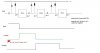
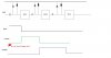
The circuit: When creating a timing chain, one 555 triggering the next and so fourth in order to produce a delayed high pulse at the circuits output.

What i dont understand: why the 1st 555s low output before its triggered doesnt trigger the 2nd 555 and why instead the 2nd 555 is only triggered by the falling edge of the 1st 555s output after the time period.

Hard to explain what i mean, i've attached a diagram to help illustrate.
 

Attachments

  • timing chain.jpg
    timing chain.jpg
    34 KB · Views: 172
Do you have a more accurate schematic?

What pin is the input on?
Are you using pin 3 for output?

I'm trying to get my head around it too... It's giving me a headache :confused:
 
Last edited:
It seems that these 555's are in monostable mode.
That means that Pin 2 connects to ground, which makes pin3 go high...

Isn't the cap supposed to be connected to pins 6 and 7?

Either way, I would think that 'B' would go high, because it's pin2 is held low (I think the line at the top of the diagram is ground?), because 'A' does not produce an output...

Tricky... Hope someone sheds light on this :)
 
Nothing holds pin 2 low. The resistor pulls it high.
The first 555 has a short negative-going pulse through the coupling capacitor from the input to trigger it.
The second 555 is waiting for a short negative-going pulse from the output of the first 555 to trigger it.
The short negative-going pulse comes from the output of the first 555 only when its output goes low when it times-out. Look at the timing diagram.
 
thx for replying guys.

I've attached an amended sketch (just added notes saying what ive missed out)
I didnt put in the timing R and Cs for simplicity, or the connections to ground.
The top rail is Vcc sorry i should of made the sketch more clear.

audioguru, you say:
'the short negative going pulse comes from the output of the 1st 555 only when its output goes low when it times out.'

i agree the 1st negative going pulse happens then but surely the output pin of the 1st 555 is at 0v before the 1st 555 is triggered, as i have shown, so how come the 2nd 555 doesnt trigger off of the 0v?
 

Attachments

  • timing chain.jpg
    timing chain.jpg
    41.8 KB · Views: 176
We need to see the timing components to see if the 555 is "ready" to accept a trigger pulse.
 
the timing components dont exist as this is a theoretical circuit!
Are you saying that the reason a timing chain can work and the 2nd 555 doesnt trigger on the 1st 555s low output before the 1st 555 is triggered, is because of the difference in periods? i dont understand :(

I still cant get my head around how a timing chain of 555s work, why does the next 555 inline only trigger on the falling edge of the previous 555s output pulse and not on the 0v that existed on the previous 555s output before it was trigggered?

I must be missing something obvious
 
I see what you mean.
The moment that the power is applied to the circuit then the output of the first 555 is low and the capacitor feeding the trigger pin of the second 555 has not charged yet. So the second 555 is triggered.
When the second 555 times-out then its output goes low which triggers the third 555.

The timers need to be reset when power is applied until the coupling capacitors have charged.
 
Unfortunatly that wasnt what i meant, i didnt realise there was a problem with waiting for coupling capacitors to charge. Although i suspect this almost solves what i dont understand. I can now narrow down what i dont get to a specific time: (time = 1 below)

time = 0 when power is first applied, (Vcc turns on) and no input trigger to the 1st 555 is supplied;
output of every 555 is low, the coupling capacitors are not charged so all the 555s except the 1st one are triggered.
If we dont want this then we must hold their resets low at circuit power on, for the time it takes to charge the coupling capacitors
i'm happy with time = 0

time = 1 Vcc is now on and all coupling capacitors are charged. There has still been no trigger provided to the 1st 555
the output of every 555 is low, the next 555s (ie all but the 1st 555) dont trigger because....... I dont understand why they not triggering!


time = 2 the 1st 555 recieves a trigger pulse and after time 1.1Rt1Ct1 (RtCt not shown on my diagram) the falling edge of the 1st 555s output triggers the 2nd 555 which after 1.1Rt2Ct2 triggers the 3rd 555 and so on and so fourth.

Thank you for your patience guys
 
Last edited:
At Time = 1 the output of all the 555's are low but since the input coupling capacitors are charged then the trigger inputs are high and are not triggered.
 
You really need to supply a circuit diagram. That's what circuit diagrams are for.
You are just running around in circles with all this discussion.
 
Thanks Audioguru i think i finally get how this works, i didnt understand the behaviour of the coupling capacitor.
 
Status
Not open for further replies.

Latest threads

New Articles From Microcontroller Tips

Back
Top