Continue to Site

Welcome to our site!

Electro Tech is an online community (with over 170,000 members) who enjoy talking about and building electronic circuits, projects and gadgets. To participate you need to register. Registration is free. Click here to register now.

  • Welcome to our site! Electro Tech is an online community (with over 170,000 members) who enjoy talking about and building electronic circuits, projects and gadgets. To participate you need to register. Registration is free. Click here to register now.

Window comparator

Status
Not open for further replies.

kpr123

New Member
I am using LTC1040 for the window comparator purpose. I am trying to simulate it in LTspice.
My Supply is 39.2V. The upper limit is 39.2V and lower limit is 24V. I brought the supply voltage down to 3.92V so as to compare with the reference voltages 3.92V(39.2) and 2.4V(24) by potential divider.
Below you can see the Schmeatic and the output at Aout as well.
As per the logic it is not working out . I cannot understand where I am wrong. Please let me know if the selected inputs(A1+,A1-,B2+,B2-) are correct or need any change.
I am attaching schematic,output waveform and asc file. Please help me out
Thank you.
 

Attachments

  • ltc1040.png
    ltc1040.png
    21.3 KB · Views: 108
  • 1040.asc
    2.5 KB · Views: 92
  • 1040fa.pdf
    222 KB · Views: 106
  • graph.png
    graph.png
    18 KB · Views: 110
It's because half your inputs are disconnected.

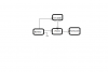
This opamp has differential inputs (two pins per input that reference each other). Regular op-amps, have single-ended inputs (one pin per input that references ground) Each differential input consists of a +/- pair of pins.

https://www.maximintegrated.com/en/app-notes/index.mvp/id/1108

As you have wired it, it's like wiring just the inverting or non-inverting input on a regular-op-amp and amp and leaving the other input hanging. If you don't need the differential part of the input, then you will have to use a resistisve divider or direction connection to a voltage source to bias one of the differential connections on each input pair.

This next part is unclear to me, but it looks as though either A or B pair can be treated as the inverting or non-inverting input by virtue of the fact you can wire the feedback up to either the + or - pin in each pair.
--------
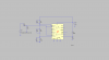
If you don't understand what I'm saying, then play around with this:
Move one connection on each op-amp to somewhere other pair of inputs. Connect all remaining unconnected input pins to either:

1. the same resistive divider at mid-voltage bias OR
2. directly to ground

What this should do is give all your inputs the same reference voltage. Since you aren't putting a true differential signal into your differential inputs, it means that if you reference to ground, you will lose half the dynamic range the op-amp inputs are capable of. Connecting it to a mid-voltage bias will give you the full dynamic range of the inputs. (True differential signals have both signals pairs swing above and below each other, but your input signal is single-ended which means that one signal in the pair swings around the other which is at a fixed voltage. If you make this fixed voltage ground, well you lose half the range because the signal doing the swinging can't swing below ground...but if you make the fixed voltage midsupply then you don't lose any range since the signal doing the swinging can swing below mid-supply until it hits ground).

These last instructions aren't exactly the solution to your problem because I don't feel like figuring out exactly what should be wired to where, but should make it so you start seeing something that makes more sense so you can start shuffling things around the inputs until it works. If you understood the first half, then you know enough to fix the issue.

EDIT: You might be able to also just leave what you have and tie the open + inputs low, and the open - inputs high so that the op-amp outputs a lo which should cause the internal NOR gate to ignore it.
 
Last edited:
Your signal source is also 3.9V, but your upper reference is also really close to 3.9V. Not the best choice for a test signal.

What is the output signal that is listed in your graph? This op-amp has three possible ones.

If you are trying to use the NOT(A OR B) output, then you have some your comparison directions reversed.

Because as you have it wired, there is no unique meaning (I assume either the signal is between MAX and MIN, or signal is beyond Max or Min) for when the NOT(A OR B) = TRUE, but true is the only unique state in that expression.

For between limits = true:
Both comparators must individually evalute to false when they are within the limits.
 
Last edited:
Here's the circuit connected as a window comparator per page 9 in the data sheet (data sheets are a marvelous invention :rolleyes:).
I changed the input to a ramp and increased its amplitude by increasing the value of R4 so you can see the window operation.
I also reduced the value of R2 to increase the strobe oscillator frequency and reduce the response time.
Edit: In real time, if the input voltage changes slowly, then a slower clock frequency will be okay, if you want it slower for some reason.

upload_2018-7-24_12-40-3.png
 
Last edited:
crutschow Thank you so much for your help. I used that circuit as a part of the undervoltage Lockout circuit. My aim is to power the hardware from battery through a pmos which acts as a switch(where the source of pmos is from battery and gate is driven by the LTC1040 (A+B)' output) like the picture below.

But I could not able to succeed in it. Could you help me out.
Thank you
Please find the attachment of schematic
 

Attachments

  • Untitled.png
    Untitled.png
    5.4 KB · Views: 90
  • 1040.asc
    3.5 KB · Views: 85
But I could not able to succeed in it. Could you help me out.
So how did it not succeed?
I see no MOSFET in the 1040.asc circuit.

I think you posted the wrong 1040.asc circuit, which is also the name of the test fixture circuit.
Give your .asc file a new name to avoid confusion.
 
The MOSFET doesn't turn off because the gate voltage has to go to the battery voltage (Vb) to turn off, and the /A+B output only goes to 5V.
I added a MOSFET level shifter M2, to get the needed gate voltages.

upload_2018-7-25_1-0-3.png
 
crutschow Thanks again. But the limit of the Vout has been changed from 28V to 16V(originally 39,2 and 24V). Is there any thing we can do to rectify this problem?
 
crutschow Thanks again. But the limit of the Vout has been changed from 28V to 16V(originally 39,2 and 24V). Is there any thing we can do to rectify this problem?
Change the value of the input resistors and/or the values of R1, R5, and R6.
How did you originally select those resistor values?
 
crutschow .As you have mentioned I have adjusted the resistor values to the requirement(please find the attachment) and now the circuit is working as expected. Now my question is how can I protect the gate of pmos and why does it need to be protected? Is it because of the Gate voltage pf Pmos?
Thank you.
 

Attachments

  • 1040.asc
    4 KB · Views: 86
May I know why did you used a 20K resistor?
Just a convenient arbitrary value.
Now my question is how can I protect the gate of pmos and why does it need to be protected?
The maximum Vgs of most MOSFETs is ±20V (from data sheet) so you must limit the voltage to below that value.

To do that, connect a 10-15V zener from M1's gate (anode) to its source terminal (in parallel with the 20kΩ already there). Also add a 10kΩ resistor in series with the drain of M2 and the gate of M1.
That will limit that Vgs voltage to 12V.
 
Status
Not open for further replies.

Latest threads

New Articles From Microcontroller Tips

Back
Top