Continue to Site

Welcome to our site!

Electro Tech is an online community (with over 170,000 members) who enjoy talking about and building electronic circuits, projects and gadgets. To participate you need to register. Registration is free. Click here to register now.

  • Welcome to our site! Electro Tech is an online community (with over 170,000 members) who enjoy talking about and building electronic circuits, projects and gadgets. To participate you need to register. Registration is free. Click here to register now.

Where to look for damage after an electrolytic leakage?

Status
Not open for further replies.

gkmaia

Member
Hi,

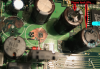
I bought a Leader Model 300 with an electrolytic leakage all around the power supply area. The device has yellowed and was probably exposed to sun and heat for a long period. And I suspect the device was used for a long time while with leakage. All electrolytics around the power supply are have been replaced and traces reconstructed.

Some background:

I am attaching images of the main board (top and bottom). Attached to the main board are separate boards. One for the DMM, another for the Oscilloscope and another for the display and buttons.

All functions on the Oscilloscope board have been restored after the fix. But the DMM is still unresponsive. If I select DMM the screen goes blank and the device freezes. CN5 is what leads to the DMM board.

After removing the electrolytics I checked each of them for shorts, none had at the moment I tested. But all of them had almost zero capacitance left.

My question then is: After a long time leakage like this one what are the components most likely to be damaged? Is there anywhere to go from here to try pin point the DMM issue? Or that is probably a lost case?

Note: I do not have a service manual

Screen Shot 2019-01-02 at 9.31.18 AM.png

Screen Shot 2019-01-02 at 9.41.04 AM.jpg
 
Last edited:
First pic: copper cladding looks rough, but serviceable. Noted caps don't look right, but they are out of focus somewhat...
1546376500217.png

Second pic: not sure what you're showing us... (don't see any damage and the colored lines aren't labeled).

Can you isolate the power connection(s) for the DMM? If so, have you checked to see what power is there?
 

Attachments

  • 1546376263836.png
    1546376263836.png
    716.9 KB · Views: 66
The caps you think dont look right are the ones removed that caused the leak. The image shows the damage they made.

Please scroll all the way down as I added a few photos.

If you look at the image you did not understand, that was the back of the main board.

Here you see traces restored.
IMG_3928.JPG


The image bellow is the DMM board (AD6303DMM) on the left where the CN4 leads.
DMM CN4 is the connection to the main board's CN5.
When DMM is on you can see there is a change in voltage on pins 16-20.
The table on the side shows where both connectors lead and voltages on each pin.
final3.jpg
 
Keep in mind that, given the density of this board, it is most likely a multi-layer board. Some traces in between layers may have been damaged. Also, if the caps had internal shorts, anything on the board could have gotten fried!
 
Keep in mind that, given the density of this board, it is most likely a multi-layer board. Some traces in between layers may have been damaged. Also, if the caps had internal shorts, anything on the board could have gotten fried!

Traces between layers around the damaged area have been checked and fixed where needed.

I did check each cap for short after removing them and none had a short. Not sure if they had shorts previously.

Yes, anything could have fried. The things is what is the troubleshooting approach to find what has fried?! Where to look first?

Or most technicians would just gave up to such task of finding what is fried?
 
Keep in mind that, given the density of this board, it is most likely a multi-layer board. Some traces in between layers may have been damaged. Also, if the caps had internal shorts, anything on the board could have gotten fried!

Multilayer boards are common but, the epoxy and solder are great protectors. I doubt any traces are damaged in inside layers (if inside layers exist).
 
I doubt it too, but there's always vias that can get eaten away.
I'm wondering how he checked for continuity between layers without a schematic.
 
Traces between layers around the damaged area have been checked and fixed where needed.

I did check each cap for short after removing them and none had a short. Not sure if they had shorts previously.

Yes, anything could have fried. The things is what is the troubleshooting approach to find what has fried?! Where to look first?

Or most technicians would just gave up to such task of finding what is fried?

Technicians work on boards that cost way more than their salary. If this is going to take two weeks to reverse engineer and develop a test protocol, and a technician and his work space costs $75 to $100/hr, then it better be an expensive board if you want to fix it (and risk a reduced service life because of the previous damage).

Good luck, it you can't quickly clean it, cut, place and solder some repair copper foil stock, add new caps and fire it up, I doubt going into more detail repair is worth the effort but, it may also be a board for a machine that makes a million dollars of product a minute and no longer available. Who am I to judge?
 
I doubt it too, but there's always vias that can get eaten away.
I'm wondering how he checked for continuity between layers without a schematic.

Vias are pretty robust too. The viscous electrolyte doesn't make its way everywhere.
 
Technicians work on boards that cost way more than their salary. If this is going to take two weeks to reverse engineer and develop a test protocol, and a technician and his work space costs $75 to $100/hr, then it better be an expensive board if you want to fix it (and risk a reduced service life because of the previous damage).

Good luck, it you can't quickly clean it, cut, place and solder some repair copper foil stock, add new caps and fire it up, I doubt going into more detail repair is worth the effort but, it may also be a board for a machine that makes a million dollars of product a minute and no longer available. Who am I to judge?

It is not about the cost of the board. I could buy another for $100. It is about the challenge. I wont mind if it takes 6 months to learn how to fix this. More I investigate, more I learn about electronics. That is the value of it. Learning.
 
I doubt it too, but there's always vias that can get eaten away.
I'm wondering how he checked for continuity between layers without a schematic.

Layers are translucent. And for the record, it does not have a mid layer. Just 2 layers. With a 25x magnifier, good backlight and lots of patience, and some components removed you can follow the traces and see where they communicate between sides.
 
Status
Not open for further replies.

Latest threads

New Articles From Microcontroller Tips

Back
Top