Triode
Well-Known Member
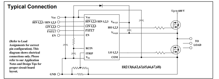
I'm looking at example layouts for the IRF2136 gate driver. Most of them are pretty similar. Here is the typical connection from the data sheet.

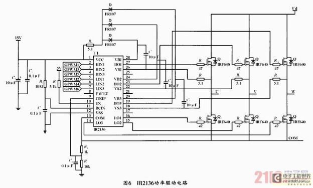
Here's one of the better complete layouts I've found

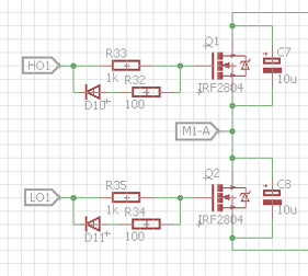
But some people's designs do this on the connection to the gates:

LO and HO go straight to the Gate driver pins. I recognize that Diode and 100 ohm resistor as a kind of snubber circuit. If it were to protect the driver chip I would think the diode would face the other way. So my best guess is that this is to allow the FET to turn off faster by letting more current flow when the driver starts pulling it low.
Any insights on this?
Thanks!
Here's one of the better complete layouts I've found
But some people's designs do this on the connection to the gates:
LO and HO go straight to the Gate driver pins. I recognize that Diode and 100 ohm resistor as a kind of snubber circuit. If it were to protect the driver chip I would think the diode would face the other way. So my best guess is that this is to allow the FET to turn off faster by letting more current flow when the driver starts pulling it low.
Any insights on this?
Thanks!
