Continue to Site

Welcome to our site!

Electro Tech is an online community (with over 170,000 members) who enjoy talking about and building electronic circuits, projects and gadgets. To participate you need to register. Registration is free. Click here to register now.

  • Welcome to our site! Electro Tech is an online community (with over 170,000 members) who enjoy talking about and building electronic circuits, projects and gadgets. To participate you need to register. Registration is free. Click here to register now.

What could be the source of noise in this resonator?

Status
Not open for further replies.

riccardo

Member
Hello,

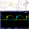
I have a simple (parallel LC, air core) resonator circuit which works well, but when I look at the scope traces of the output waveform, there's quite a bit of noise. (Picture attatched).

I have the scope connected between GND at the input, and each of the output terminals.

I've tried adjusting some resistor values and so on, but it stays more or less the same, or just does not resonate.

Another thing I noticed is that using a different MOSFET can alter the output too. For example, using a BUK7613, it will draw around 3A while resonating, whereas if I use an STP60NF10, this rises to about 5A. I suppose this could be due to the speed causing more cross conduciton.

Is there anything obious in the diagram, or does that noise waveform look familiar to anyone?
 

Attachments

  • resonator.png
    resonator.png
    98.8 KB · Views: 180
Last edited:
It could be resonance in the inductor, the connecting wires, or even the gate drive circuits.

What do the waveforms on the FET gates look like?

Without a tuning cap directly across the output coil to set it to the switching frequency, there could be resonances in many places.
 
If the o/p is a seperate winding it too can have its own snubber.
Under load it may not be so bad.
 
The circuit is self resonant a bit like a Royer oscillator. The large sine waveform is the resonant frequency of the load which is about 10 turns of copper with about 2uF of parallel capacitance.
The gate waveform does also show some of that higher frequency but due to it being a self resonating circuit I am not sure if the noise is coming from gate drive, or from the MOSFET/Load, which is then just copied back to the drive circuit.
 
Something is resonating. I think it is the 100uh coil at the center tap. I can't tell if you have two FETs on for a shout time or no MOSFETs on but the coil thinks you changed the current sharply.
 
To start with, change the gate resistors to eg. 4.7 ohm.
You are using driver rated at four amps. 4.7R it reasonable even with the maximum 18V supply to that device.

The zener diodes on the NAND spare inputs are pointless, but do no harm.

An adjustable non-overlap drive circuit may be advantageous to improve crossover timing, as Ron says.

It should also really have some filtering in the feedback / control part to prevent unduly fast changes in drive signal.
 
"To start with, change the gate resistors to eg. 4.7 ohm. "
When I do this, it seems to lock on and resonate at some very high frequency and with a strange waveform. I think in this case the parasitics are ending up driving the main resonance. 47R was about as low as I could get away with and have it oscillate properly.

"The zener diodes on the NAND spare inputs are pointless, but do no harm. "
I replaced the zeners with 500pF capacitors and that reduced the noise amplitude a decent amount. I tried increasing to 1nf, but then it began oscillating like mentioned above.
 
OK, your diagram does not show the circuit that controls the inputs to the NAND gates.

We need to see that to understand how the overall thing is working.

The oscillation must be due to the crossover timing between the two FETs; without some actual control there, they are conflicting in some way when the drive signals are to sharp.

Connect the spare input on each NAND gate to the output of the opposite one, to start with. That makes it impossible for both FETS to be driven on simultaneously.

It will still need other mods, depending on the circuit feeding them.

It's all there in the diagram. Check the net labels
 
OK, it's just drawn in an unusual way that makes it appear there are external connections...

I need to think about that a bit more, it's a can of worms as it is.
 
Status
Not open for further replies.

Latest threads

Back
Top