Ron H said:
e-l-e-c-t-r-o said:
Ron H said:
The trouble with the dual slope integrator is that, IMHO, you dont have time to do it. It requires counters and logic (or something like a PIC) to implement it. And an op amp integrator is a MUCH better way to do it. See **broken link removed**.
Regarding your last post - If you clamp the input voltage to zero, what is going to cause that clamp to be released? Are you going to do it with a mechanical (pushbutton) switch, or does it release after a fixed period of time, or... :?:
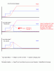
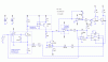
As the graph indicates, the clamp-release occures after "change of condition between in/out voltage levels".
You can see that the clamp condition starts when the output (capacitor voltage) gets greater than input voltage.
The clampl of both in/out occurs until the point where the output becomes less than the input.
Of course, that operation requires the input voltage to be clamped much more drastically than the output 8)
Is that possible? :roll:
I don't think you understand my question. Where does your input voltage come from? When the input voltage gets clamped, it doesn't go away, like the charge on the cap does when it gets discharged. The input voltage is still there - it is just "disconnected" from the input. If you release the input clamp as soon as the cap discharges, the cap will start to charge again. Then you have an oscillator, as we have discussed. If, on the other hand, you latch the input clamp, you will need some sort of external stimulus to reset the clamp.
I think the key point I'm trying to make is that the input voltage is (in my mind) an independent control voltage. If it goes to zero when you clamp it, how does it assume a non-zero value some finite length of time later?
Oh, let me see if I got your question :?
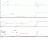
The input signal I designed in the graph we can assume to occur due to another signal before it.
Meaning, that dc voltage variation could come from a signal before it that has a fixed time of occurence (this is why I reffered to the system as "one-shot"); let's say 15ms.
For example, it may be an analog sine wave. :shock:
The sine wave could have different peak levels that are converted into relative DC signals (not same levels' conversion-just relative; But I don't know if that is possible

).
So, the real problem would be that the DC converted signal has infinite time of occurence, while the signal before it has a finite time (15ms).
In addition, a second finite sine wave can occur only after 30ms from the first (we set this as a "rule of thump", cause it simplifies the way the clamp could be released).
Considering all the above, I think the simplest (if not the only) way to go is by setting a fixed time period for the external stimulus to reset the clamp.
Assuming the input signal takes its maximum level in no more than 15ms, then the capacitor discharges around the 25th millisecond. :idea:
So, the input can be stopped to be clamped after the 26st millisecond 8)
The circuit could understand IF & WHEN an input clamp has occured, and release the clamp after a fixed period of time.
(The trick in such operation success is a "rule of thump" we can set:
That the input lasts for 15ms, and another input signal can occur only after 30 ms from the first one. 8) )
Now, the big question is of course HOW that can be done :roll:
Despite of designing the exact operation, which I am sure you can do far better than me,
I think another base in deciding
not to reset the clamp while the capacitor is discharging could be the one I mentioned in my previous post:
the circuit's ability to compare the input/output levels, and be aware when the one becomes greater than the other. :shock:
In plain English, the circuit should understand that an input clamp has occured, and decide not to release that clamped until the output level becomes less than input one.
Summary: The whole concept is that a "one-shot" input occurs (i.e a sine wave), convert its peak fluctuations into (relative) DC level fluctuations, then charge a capacitor linear to produce a "one-shot" sawtooth waveform, while clamping both DC level and capacitor voltage so that a second "one-shot sine wave" can occur after a certain before of time from the first. 8)