Continue to Site

Welcome to our site!

Electro Tech is an online community (with over 170,000 members) who enjoy talking about and building electronic circuits, projects and gadgets. To participate you need to register. Registration is free. Click here to register now.

  • Welcome to our site! Electro Tech is an online community (with over 170,000 members) who enjoy talking about and building electronic circuits, projects and gadgets. To participate you need to register. Registration is free. Click here to register now.

Using Timer1 in 16-bit mode.

Status
Not open for further replies.

Peet19

Member
HI everyone!
I would like to ask how the timer1 counter registers should be written in 16-bit mode?
I looked at Microchip's help document, but I don't fully understand it. I set RD16 in T1CON to 16-bit mode, but even then the code does not work as shown in the picture.
How should this 16-bit register be written?
Thank you in advance for your help!
 

Attachments

  • RD16.png
    RD16.png
    25.7 KB · Views: 156
You forgot to mention which processor you are talking about. Generally speaking, there is a particular order for writing the two bytes. This should usually be done in such a way that an interrupt is not possible between the two writes. Writing the 1st byte freezes the timer and writing the second by enables the timer to continue with the new value. Without knowing which processor, you are talking about, it is hard to give you a precise answer.
 
Which device?

Normally, the symbol 'F' is defined as '1' in the device header file.

The syntax of the MOVWF instruction is 'MOVWF f, a', where 'f' = file reg and 'a' is the access bit.
'a' = 0 --> Register used is in Access Bank, 'a' = 1 --> Register used specified by BSR Bank Register

So, you're specifying to use the banksel register. Is it set to the same bank as TMR1L/TMR1H?

On all the 8-bit devices, in 16-bit mode you write the high byte first (TMR1H), and then the low byte (TMR1L). Read is done in the reverse order.
 
It is a PIC18F24K22.
There is not a problem specifically with access to the registers. I can write the TMR1H and TMR1L registers, but only separately.
Ex: MOVLW 1
MOVWF TMR1H
MOVLW 2
MOVWF TMR1L
However, if it is in 16-bit mode, I can only write in the same way as if it were in 8-bit mode.
I don't see the difference between the two.
If I want to read or write, the lower and upper bytes must be written separately, since W is only 8 bits.
What is the difference between the two?
 
MOVWF TMR1H is not the same as MOVWF TMR1H, 1 which is what you have with 'F' = 1
The first one assumes that the 'a' access bit is 0, while the second one says to use the BSR.

Either add a BANKSEL TMR1L or drop off the ', F' and see if it works.
 
The high byte cannot be read or written but a copy of it can. The value is transfered to the real TMR1H when the low byte is read or written. If you keep that in mind then the sequence (high first on write etc.) makes sense.

Mike.
 
I set RD16 in T1CON to 16-bit mode, but even then the code does not work as shown in the picture.

There is not a problem specifically with access to the registers. I can write the TMR1H and TMR1L registers, but only separately.

Which is it? The first statement says it doesn't work, the second says you don't understand the datasheet.
 
Thanks, I'll try as you wrote.
I understood the question to mean that if it is in 16-bit mode or if it is in 8-bit mode, the TMR1H and TMR1L registers must be written in the same way. I don't understand the difference. The image in the example shows that TMR1L is also written across TMR1H, but this did not work for me.
However, I can write the registers separately.
As my previous reply - READ THE DATASHEET - it explains everything, I even gave you the page and section number.
 
The datasheet does indeed explain it but I've found on numerous occasions that posters seem to me incapable (or too lazy) to read them. I tried (in vain it appears) to explain it in simple words but that didn't work either.

Mike.
 
The image in the example shows that TMR1L is also written across TMR1H, but this did not work for me.
I don't know where you got the example in post #1, but as I explained in post #3 that example is wrong in that the instructions to load the TMR1 registers use the BSR but it never shows setting it. Also, there's no reason to clear the TMR1L register first... with RD16=1 both TMR1H and TMR1L will get updated at the same time.
 
Jeez, I need new glasses!
The example in post #1 never updates TMR1L... it writes to TMR1H twice! That's another reason for it not to work!

Just use the method from your post #4. That'll work in both 16-bit and 8-bit modes (as long as TMR1H/TMR1L are in the access bank). If the TMR1 regs are in another bank then add a 'banksel' and that way it'll always work
Code:
BANKSEL TMR1L
MOVLW 1
MOVWF TMR1H
MOVLW 2
MOVWF TMR1L
 
I see your confusion. That's from a VERY old app note (1997) before they added the latched 16-bit mode (there's no RD16 bit in the T1CON control register in that app note). Even so, that example obviously has issues.

Always best to check the datasheet for the device you're using.
 
It all seems pretty straightforward, the datasheet information is below:

Code:
12.6 Timer1/3/5 16-Bit Read/Write Mode
Timer1/3/5 can be configured to read and write all 16
bits of data, to and from, the 8-bit TMRxL and TMRxH
registers, simultaneously. The 16-bit read and write
operations are enabled by setting the RD16 bit of the
TxCON register.
To accomplish this function, the TMRxH register value
is mapped to a buffer register called the TMRxH buffer
register. While in 16-Bit mode, the TMRxH register is
not directly readable or writable and all read and write
operations take place through the use of this TMRxH
buffer register.
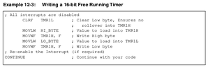
When a read from the TMRxL register is requested, the
value of the TMRxH register is simultaneously loaded
into the TMRxH buffer register. When a read from the
TMRxH register is requested, the value is provided
from the TMRxH buffer register instead. This provides
the user with the ability to accurately read all 16 bits of
the Timer1/3/5 value from a single instance in time.
In contrast, when not in 16-Bit mode, the user must
read each register separately and determine if the
values have become invalid due to a rollover that may
have occurred between the read operations.
When a write request of the TMRxL register is
requested, the TMRxH buffer register is simultaneously
updated with the contents of the TMRxH register. The
value of TMRxH must be preloaded into the TMRxH
buffer register prior to the write request for the TMRxL
register. This provides the user with the ability to write
all 16 bits to the TMRxL:TMRxH register pair at the
same time.
Any requests to write to the TMRxH directly does not
clear the Timer1/3/5 prescaler value. The prescaler
value is only cleared through write requests to the
TMRxL register
 
Status
Not open for further replies.

Latest threads

New Articles From Microcontroller Tips

Back
Top