Continue to Site

Welcome to our site!

Electro Tech is an online community (with over 170,000 members) who enjoy talking about and building electronic circuits, projects and gadgets. To participate you need to register. Registration is free. Click here to register now.

  • Welcome to our site! Electro Tech is an online community (with over 170,000 members) who enjoy talking about and building electronic circuits, projects and gadgets. To participate you need to register. Registration is free. Click here to register now.

The Spike in Question :(

Status
Not open for further replies.

lord loh.

Member
Here is a circuit that is a part of my project. The problem is the two spikes that I just cannot explain.

I am as much intrested in knowing why they are there as much as getting rid of them.

Please Help.

Thank you.
 

Attachments

  • ckt_201.gif
    ckt_201.gif
    12.4 KB · Views: 428
  • graph_366.gif
    graph_366.gif
    7.8 KB · Views: 415
  • pd-project.zip
    1.2 KB · Views: 127
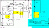
When input1 goes high, the voltage at the output of your NOR gate drops because Q2 turns on. This voltage couples back through the collector-base capacitance of Q1, causing the spike on input2. The problem is caused by the fact that you are using two nuclear bombs (2N3055, which has huge junction capacitance) to kill a mosquito. Change the transistors to any small-signal part (e.g. 2N3904), and the problem will go away. You don't need R3 and R4. R1, R2, and R9 can be at least 10 times larger. Your base resistors can be 10 to 20 times the parallel resistance of R1 || R2 || R9. Also, your timing resistor (R8) can be any value up to 100k, allowing you to use a smaller value for your timing capacitor.

The spike will still be there to some extent. You can clip it off with a 1N4148 from base to GND, anode to GND, if it bothers you. You should have one on each base, although I wouldn't worry about it. Base-emitter breakdown voltage on most transistors is at least 5 volts.
 
You are learning a lot about junction capacitance. :D
The pulse is coupling through the diode junction capacitance. A smaller diode will help, but you'll still get a big pulse (on the simulation). I think the 555 actually has a diode from each pin to VCC, for esd protection. The usual scheme for limiting the spike is as in the schematic below. Note that I also changed the base resistors and the timing components.

Also, here is a model for BC547B.
Code:
.MODEL BC547B NPN( IS=2.39E-14 NF=1.008 ISE=3.545E-15 +NE=1.541 BF=294.3 
+ IKF=0.1357 VAF=63.2 NR=1.004 ISC=6.272E-14 NC=1.243 BR=7.946 IKR=0.1144 VAR=25.9 
+ RB=1 IRB=1E-06 RBM=1 RE=0.4683 RC=0.85 XTB=0 EG=1.11 XTI=3 CJE=1.358E-11 
+ VJE=0.65 MJE=0.3279 TF=4.391E-10 XTF=120 VTF=2.643 ITF=0.7495 PTF=0 
+ CJC=3.728E-12 VJC=0.3997 MJC=0.2955 XCJC=0.6193 TR=1E-32 CJS=0 VJS=0.75
+ MJS=0.333 FC=0.9579)

You can copy and paste this into the standard.bjt file (in LTC/SWCADIII/lib/cmp). You can do this with any model.

BTW, the sim will run lightning-fast if you eliminate the maximum time step and let SWCAD select the time steps as it sees fit.
 

Attachments

  • pd-proj_mod.png
    pd-proj_mod.png
    19.2 KB · Views: 370
Why not simply use a NOR gate IC and a monostable IC? Examples - the CMOS 4001 NOR and the 4528 Mono.

This would significantly reduce the number of components. And the output from the NOR can be connected directly to the input of the mono, ie. you won't need the capacitor.

I have not checked the data sheet of the 4528 so I don't know whether it triggers on the positive or negative edge (some give both options).

But you will have 3 spare NOR gates, one of which could be used as an inverter if necessary.
 
Here is how you model switches. Read about the SW element in the help file. If you want to keep the transistors, you can still model the switches driving them.
 

Attachments

  • pd-proj_mod1.png
    pd-proj_mod1.png
    17.7 KB · Views: 365
Status
Not open for further replies.

New Articles From Microcontroller Tips

Back
Top