Continue to Site

Welcome to our site!

Electro Tech is an online community (with over 170,000 members) who enjoy talking about and building electronic circuits, projects and gadgets. To participate you need to register. Registration is free. Click here to register now.

  • Welcome to our site! Electro Tech is an online community (with over 170,000 members) who enjoy talking about and building electronic circuits, projects and gadgets. To participate you need to register. Registration is free. Click here to register now.

SPI & nRF24L1+ help please!

Status
Not open for further replies.

olly_k

Member
Folks, is there anyone here, who fully understands how to talk to these modeles. Not interested in some kid who has stuck a load of modules on an arduino written by someone else together, but someone who has actually written everything from scratch, or at least fully understands how to get these things to chat.
I am not finding the manual absolutely clear as to the finer details, which I suspect I am missing something (or my modules are really dodgy Chinese rips!)

Basically, I have written an SPI routine (never done this before) in assembly for a PIC16f688 and I am fairly happy with it. You enter data in to 4 registers initially, two that contain where to raise CSN, (which are rotated end of each group of clock cycles) then the number of writes in another register, number of reads in a further register, then it's a case of just entering up to 15 addresses / data's and the code does the rest to produce SPI (at the moment, phase and pol are 0-0). MOSI is rotated out of registers 0x6X and in to the end. Thus it is kind of FIFO.

SO I think I have got that bit right. I have got everything moving slowly, as I am based on breadboard for now.

Good News, I do I get a MISO response from the RF unit. Bad news, I can't really seem to make much sense of it or control the modules! I am obviously overlooking something.

I will try to get a trace at work tomorrow, but for now below is an MPLAB sim of the data sent out without obvious MISO, which, like I said above, I do get.

I have skipped the majority of config in this example as I thought I would show how I am setting a receive address in Data Pipe 0. I am sending [CSN LOW] 0x0A followed by 0xAA 0xAA 0xAA [CSN HIGH]. clock is approximately 500uS each cycle, 1mS rest between each byte of data, CSN highs are 760uS. At the end of transmitting this I then set to expect 3 bytes in RX_PW_P0 with [CSN LOW] 0x11 0x03 [CSN HIGH]. You can see the CE pin going high at the far end too.

The MISO data I am getting back I am struggling to understand, and I have tried transmitting (I put it off as long as I could!) to no avail.

Please can someone put me out my misery and shine some light on where I might be going wrong!!!?

Thanks.

*Managed to get old scope behaving (nearly) so you can see the output! MISO is showing 0x0E although in this case I have not set any config registers other than you can see. Will address that tomorrow as I am tired!
 

Attachments

  • Data sent.jpg
    Data sent.jpg
    158.6 KB · Views: 97
Last edited:
It would help if you labelled the simulation and the traces.

There could be something different happening at the last clock bit of the first byte. If the clock isn't changing cleanly it may be seen as more than one pulse.

What are you trying to send to the nRF24L01+ ? . The commands are on page 51 of this:-
https://www.nordicsemi.com/eng/cont.../file/nRF24L01P_Product_Specification_1_0.pdf

I think that you should be sending 0x2A in the first byte, so in binary 00101010. Commands that start 001 are to write to an address, while commands that start 000 are to read the address. You sending 0x0A, so in binary 00001010, so that reads register 0x0A, and the answer from the nRF24L01+ appears to be 0xE7E7E7, which is the first three bytes of the default for register 0x0A, as it says at the bottom of page 59 of that data sheet. Only 3 bytes were sent by the nRF24L01+ as CSN was taken high after that.

Also, I suggest you avoid receive addresses like 0xAA AA AA. It is really easy to get you or the data receiver confused as to where the bytes start and finish in a data string that is only alternating 1s and 0s. I would used something like 0x90 A5 0F (binary 1001 0000 1010 0101 0000 1111) just to break things up a bit.
 
Thank you Mike, I had completely overlooked that bit! I will make the change, write, then read in the same manner, and change the values to something a little less ambiguous. The AA string was only ever for test purposes to be honest, will have individual commands in finished idea!

Regards the glitch, the scope is old, it was far worse before but I tried one last time. I will use our works one soon.


Quick question then, I assume this 0x2# applies equally before writing to Config too! - How stupid I feel, not sure I'd have figured this out!

I have read a lot of manuals, but something about this one wasn't terribly clear to me!


It would help if you labelled the simulation and the traces.

There could be something different happening at the last clock bit of the first byte. If the clock isn't changing cleanly it may be seen as more than one pulse.

What are you trying to send to the nRF24L01+ ? . The commands are on page 51 of this:-
https://www.nordicsemi.com/eng/cont.../file/nRF24L01P_Product_Specification_1_0.pdf

I think that you should be sending 0x2A in the first byte, so in binary 00101010. Commands that start 001 are to write to an address, while commands that start 000 are to read the address. You sending 0x0A, so in binary 00001010, so that reads register 0x0A, and the answer from the nRF24L01+ appears to be 0xE7E7E7, which is the first three bytes of the default for register 0x0A, as it says at the bottom of page 59 of that data sheet. Only 3 bytes were sent by the nRF24L01+ as CSN was taken high after that.

Also, I suggest you avoid receive addresses like 0xAA AA AA. It is really easy to get you or the data receiver confused as to where the bytes start and finish in a data string that is only alternating 1s and 0s. I would used something like 0x90 A5 0F (binary 1001 0000 1010 0101 0000 1111) just to break things up a bit.


Not sure if that would help to be honest, and not sure if I am terribly proud of my code, but if you really have to....
 
We start by putting first byte in to the out buffer, then subsequent bytes in to registers defined by a start address, FSR resumes thereafter.
We then enter number of reads, number of writes and the pattern for CSN
We call CALCFCNT to re-adjust above figures (this was a whim and not like I am struggling for space!)
Then call SPIGO to actually send the data.
It's slow, it's clunky, but it is mostly automated and works. I will probably take a more shopping list approach if I need speed, or choose a pic with build in SPI which would be a lot less hassle!

Oh and the FSR routine does a bit of everything really, whatever I was so is quite durable I think.

All code (C) Olly_k 2018 
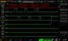
;=================================SPI ROUTINE================================= CLKH: btfss INTCON,T0IF ;Check if time for a change goto $-1 bcf INTCON,T0IF ;Reset flag bsf PORTC,CLK ;Clock High return CLKL: btfss INTCON,T0IF ;Check if time for a change goto $-1 bcf INTCON,T0IF ;Reset flag bcf PORTC,CLK ;Clock High return ;-------------------------------------------------------------------- CALCFCNT: ;We calculate the value to put in to fsrCNTin ;Which decides how many rotates for the buffer shuffle ;We assuming tempS1 still in working at this point too! subwf tempS0,w ;Here is stored # of MOSI btfss STATUS,C goto $+8 btfss STATUS,Z ;If both data the same we must set flags goto CALC goto $+5 CALC: movf tempS0,w movwf fsrCNTin bsf SPIflgs,7 ;TEST return movf tempS1,w bcf SPIflgs,7 ;required? movwf fsrCNTin return SPIGO: ; registers to temp registers movf FsRrADin,w ; movwf FsRrADDY movf fsrCNTin movwf fsrCNT ; Pre-initialisation - MISO starts off clear, so we can put 0x01 in to file ; and wait for it to come round. ; MOSI requires a seperate counting reg (SPIbit) SPICNT0: movlw 0x01 movwf SPIbufI ;Preload input with 0x01 for 'byte full' test movlw 0x08 ;This is for READ movwf SPIbit bcf PORTC,CSN ;CSN LOW any data from now on is valid bcf INTCON,T0IF ;Let's start the timing over bsf SPIflgs,4 ;First time we want to reset TMR count. ;-----------------------SPI LOOP------------------------ SPILP: ;This is the SPI Loop, lets roll the data in to STATUS ;But first, Check for data to roll out. btfss SPIflgs,1 ;Is there still anything to send? goto CTL ;Yes ;CONT... movlw 0x01 movwf fsrCNT btfss SPIflgs,2 ;Is that it now nothing for MISO? goto SPIOUT ;CONT... movf fsrCNTin,w movwf fsrCNT btfsc SPIflgs,7 goto $+2 goto SPIret ;TEMP TEMP bsf FSRflgs,3 call FSRrtn ;ONE LAST SHUFFLE goto SPIret ;exit routine ;Here we now start to rotate and read the output buffer (SPIbufO) CTL: rlf SPIbufO,f ;Lets get the first value to output from MOSI btfss STATUS,C ;1 or 0? goto SPIoutL ;Go to SPIoutLOW ;CONT... SPIoutH: bsf PORTC,MOSI goto SPIOUT SPIoutL: bcf PORTC,MOSI SPIOUT: bcf PORTC,CSN btfss SPIflgs,4 ;Is this the first clock pulse? ;If so, we want a nicely timed first pulse ;So we reset TMR0 goto $+5 ;Not our first time ;CONT... movlw 0x00 ;Set TMR0 for a full count movwf TMR0 bcf INTCON,T0IF bcf SPIflgs,4 ;************************* call CLKH ;Action the Output to the bus! ;************************* ;Now we have sent data we need to collect ;But first, lets see where we are up to! MOSi: btfsc SPIflgs,1 ;Test if still to check for data output goto MISo decfsz SPIbit,f ;SPI bit cnt, when out 8 bits check more bytes? goto MISo ;Nothing to worry about, continue ;***********TEST1 bcf STATUS,C rlf tmp3,f ;Do we want a delay and if so is it time? rlf tmp,f ;rotate previous carry if there is one btfss STATUS,C goto MOSCNT bsf SPIflgs,3 ;Set delay flag ;CNT... MOSCNT: ;***********TEST1 movlw 0x08 movwf SPIbit decfsz tempS0,f ;Check and dec number bytes goto MOcnt ;Continue bsf SPIflgs,1 ;We set flgs,1 to inhibit further reads goto MISo ;We now need to shuffle all registers MOcnt: bsf SPIflgs,0 ;We need to shuffle everything but not yet ;Set up addys again for next shuffle MISo: btfsc SPIflgs,2 ;Have we finished MISO? goto SPILPC ;Yes? Back to MOSI, but hang on, CLK RST! btfss PORTC,MISO ; goto MISOl ;Low, go to MISO Low MISOh: bsf STATUS,C goto $+2 MISOl: bcf STATUS,C rlf SPIbufI,f ;Rotate above carry in btfss STATUS,C ;Check if we have come round? goto SPILPC ;ok so we need to wait to cont clock bsf SPIflgs,0 ;shuffle! movf SPIbufI,w ;We need to save the file now! movwf FsRiDATA ;Ready to feed in to chain movlw 0x01 movwf SPIbufI ;Number of addresses to put in decfsz tempS1,f ;ok, byte complete, dec count goto SPILPC bsf SPIflgs,2 ;No more data to read in ; CONT... SPILPC: ;************************* call CLKL ;Action the Output to the bus! ;************************* btfss SPIflgs,1 ;ensure very LAST bit sent is cleared! goto $+2 bcf PORTC,MOSI ;Do it1 ****************ADDED THIS BELOW TEST3 CLKCNT: ;***********TEST1 btfss SPIflgs,0 ;End of byte? *+*+*+*+*+*+*+*+ Check here for byte goto SPILP bcf PORTC,MOSI ;---------------READY TO SHUFFLE FOR NEXT DATA--------------- ;THere is an option to allow the FSR shuffle to shrink as data lessens.. ;This may be required for faster code but generally remains inactive. ;Might remove or make it a feature. It looks a but messy btfss FSRflgs,4 ;Check for reduced shuffle goto $+3 movlw 0x18 ;This will set FSRflgs,4; shuffle shrink goto $+2 movlw 0x08 ;Lets set up FSR flags movwf FSRflgs ; Ok prep - copy current files in to temp before continue movf FsRrADin,w ; movwf FsRrADDY movf fsrCNTin,w movwf fsrCNT call FSRrtn ;Get next data bcf SPIflgs,0 ;reset ;-------------------PLANNED BREAK BETWEEN CLOCKS------------------ btfss SPIflgs,3 goto $+2 bsf PORTC,CSN ;*************TEST3 call DLY500uS bcf INTCON,T0IF ;Reset flag bcf SPIflgs,3 goto SPILP ;----------------------End routine SPIret: call DLY50uS bsf PORTC,CSN ;render any data invalid clrf SPIflgs return ;******************************************************************** ;******************************************************************** ;-----------------------------FSR Routine---------------------------- ;Please see file FSRRoutine.asm for instructions FSRrtn: rFSR: btfss FSRflgs,1 ;one-shot Read goto fsrWR fsrRD: movf FsRrADDY,w ;initial/current read addy movwf FSR movf INDF,w movwf FsRoDATA ;This is Data to be read out incf FSR,f movf FSR,w movwf FsRrADDY ;save new value for next increment bcf FSRflgs,1 ;Cancel read return fsrWR: btfss FSRflgs,2 ;WRITE goto fsrSHUF ;No change, set flag and exit movf FsRwADDY,w ;initial/current read addy movwf FSR movf FsRiDATA,w ;This is Data to be read in movwf INDF incf FSR,f movf FSR,w movwf FsRwADDY btfss FSRflgs,3 ;Shuffle? return. ; btfsc FSRflgs,3 ;Shuffle? return. return fsrCNt: ;if a multi byte wipe is requested we will continue ;here decfsz fsrCNT,f ;Count requested number to clear goto fsrWR ;no clear next return ;do we want to write multiple times? ;------------SHUFFLE CODE! ;Start address, FSRflag 3 set, number of shuffles set. ALL GOOD fsrSHUF: ;READ ;***Current working registers are moved to temp registers movf FsRiDATA,w movwf tempF2 movf FsRrADDY,w movwf tempF0 movf FsRwADDY,w movwf tempF1 ;First we need to read the current read ADDY and write the same movf FsRrADDY,w ;Copy the address! movwf FsRwADDY ;WRITE AND READ THE SAME ;Now copy that first buffer in to the output register bsf FSRflgs,1 ;We need a read! call fsrRD ;Back on ourselves again, for a read movf FsRoDATA,w ;We copy the first shift to buffer movwf SPIbufO ;Done; we do not come back here now ShufLP: ;This is loop x times ; First we read the file to shuffle from stored address ;sequence - as we had a read for the output buffer we ;area already 1 increment up. ; FIRST READ btfss FSRflgs,4 ;Check for reduced shuffle goto $+3 movlw 0x1A goto $+2 movlw 0x0A ;Lets set up FSR flags (00001010) movwf FSRflgs call rFSR ;Read next file movf FsRoDATA,w ;we need to copy to the next buffer movwf FsRiDATA ;The previously read file is now written to the incremented register ; WRITE FIRST READ btfss FSRflgs,4 ;Check for reduced shuffle goto $+3 movlw 0x14 ;00001000 Select one shot write goto $+2 movlw 0x04 ;Lets set up FSR flags movwf FSRflgs call fsrWR ;do it! decfsz fsrCNT,f ;Have we finished yet? goto ShufLP ;Repeat again ;Now we reduce the shuffle count and determine if any more ;shuffles are required. movlw 0x01 subwf FsRwADDY,f ;We reduce the count for next shuffle n-1 movf tempF2,w movwf FsRiDATA ;This needs to be put in shuffle train ;Also we need to reduce the write address by 1 ;TEST btfss FSRflgs,4 ;Check for reduced shuffle goto $+3 movlw 0x14 goto $+2 movlw 0x04 ;Lets set up FSR flags movwf FSRflgs call fsrWR ; movlw 0x01 addwf FsRwADDY,f ;Bump address back up clrf FsRiDATA ;TEST btfss FSRflgs,4 ;Check for reduced shuffle goto $+3 movlw 0x10 goto $+2 movlw 0x00 ;Lets set up FSR flags movwf FSRflgs CT: ;TEST btfss FSRflgs,4 ;Check for reduced shuffle goto $+3 movlw 0x10 goto $+2 movlw 0x00 ;Lets set up FSR flags movwf FSRflgs ;restore addresses movf tempF0,w movwf FsRrADDY movf tempF1,w movwf FsRwADDY return ;=========================== CheckADDY: ;So let's check to see this is ;Addressed to us. clrf FSRflgs ;we're on, no need for delay movlw 0x61 ;This is first ADDY movwf FsRrADin ;Put initial address in to FSRw clrf SPIflgs ;We clear the flags first movlw 0x01 ;ok first we are expect 16-byte MOSI writes movwf tempS0 movlw 0x04 ;We are expecting x MISO read movwf tempS1 call CALCFCNT ;Lets configue number of shuffles ;fsrCNTin IS LOADED AUTOMATICALLY call SPIGO return
 
You seem to have combined SPI code with lots of other code. I expected a routine which clocked out a byte while clocking in another.

Mike.
 
You seem to have combined SPI code with lots of other code. I expected a routine which clocked out a byte while clocking in another.

Mike.
It does exactly that Mike, but anything from 1 to 15 bytes can be clocked out or in or any combination without leaving this routine. The FSR routine is in itself separate so I could have removed from here for clarity. I did all this for apparent ease of programming so I have a small initialization and then just call the routine and it does the rest. I am sure there might have been a simpler way but I just program how I see the world so to speak. Some of my stuff probably does get a little overcomplicated though!


Can't believe how stupid I've been, although I have been up against things with this project with a few technical problems with installation to get it going. Damn. Still not getting excited yet but it's a big relief I made a stupid mistake!
#
 
ok folks, I have made some changes, attempting to program it into constant carrier mode (test) spoke nicely to someone at work with a spectrum analyser. Not seeing anyting on the output centered around 2.4Ghz with 150Mhz either side. Zilch.
THis is what I have entered, in the order of the instructions..

Config
0x20
0x52 =PWR_UP, PrimRX=0

2mS CSN high

RF REG:
0x26
0xB6 = 256kb CONT WAVE PLL LOCK PWR 00db

RF CH
0x25
0x06

Then I have set the CE pin high

I also send 0x06 and 0x05 at the end hoping to read the contents I have just entered but getting nothing back....
NewFile1cccc.jpg
 

Attachments

  • NewFile1ddd.jpg
    NewFile1ddd.jpg
    88.7 KB · Views: 78
Can I suggest you write a routine that writes 1 byte and reads one byte at the same time. Use the timing diagram on page 52 of the data sheet.

Then, when you need to write to registers, set CSN low, call the routine with the command and data bytes and then set CSN high again.

Start with a command like flush_tx that doesn't have any data and see if you get the status register returned.

I cannot follow your code above which is why I'm suggesting this.

Mike.
 
Thanks Mike, I had to walk away for a bit as it was doing my head in! Turns out there were some little niggles that needed ironing out. I am now talking to the module, getting expected response, and have even seen the output of a module on a spectrum analyser at work so things are looking positive.
As an experiment, I set up data pipe0 with 3 bytes of data, requested a check of FIFO status (x17), enabled CE for 10mS then checked status again and first time round Fifo status showed 0x01, after CE on for 10mS I get 0x11. This is great news, as it shows it has offloaded data. I just can't seem to receive anything arghhh!

Keeping things really simple, following the procedures outlined for communicating with the older non + (I am commanding many modules at once so cannot use ACK etc.) so all bits in EN_AA of 0, retrans all 0, no CRC and all data in and out of a 3-byte address assigned to pipe 0. Such a shame there is no LED that shows operation directly from the chip!

I know this has to be down to something stupidly simple now!?

BTW I do know my SPI code is bang on now, really happy with it! Might be a bit spaghetti junction but it does the job with minimal setup each time.


Can I suggest you write a routine that writes 1 byte and reads one byte at the same time. Use the timing diagram on page 52 of the data sheet.

Then, when you need to write to registers, set CSN low, call the routine with the command and data bytes and then set CSN high again.

Start with a command like flush_tx that doesn't have any data and see if you get the status register returned.

I cannot follow your code above which is why I'm suggesting this.

Mike.
 
Status
Not open for further replies.

Latest threads

New Articles From Microcontroller Tips

Back
Top