Electro Tech is an online community (with over 170,000 members) who enjoy talking about and building electronic circuits, projects and gadgets. To participate you need to register. Registration is free. Click here to register now.
Welcome to our site! Electro Tech is an online community (with over 170,000 members) who enjoy talking about and building electronic circuits, projects and gadgets. To participate you need to register. Registration is free. Click here to register now.
i like this idea. i have been applying pours to both sides of all my boards. i now have a better understanding of their purpose. ill keep the via as well
i like this idea. i have been applying pours to both sides of all my boards. i now have a better understanding of their purpose. ill keep the via as well
The real purpose is help reduce noise on the board. The lower ground pour and upper signal and power tracks form a capacitance that acts like a parasitic filter capacitor(s) and helps reduce noise. But it can also be used to this advantage.
Not the way I would have done it but it will work.
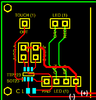
Here's a suggestion.
Add a top ground pour as shown in dashed lines. Pour becomes -V.
Then move C1 so you can connect +V trace from IC-pin5 to C1.
Pour will auto-connect IC-pin 2 and C1-ground to ground. So you don't have to manually route the track.
Do the same to the other circuit, then connect the pour(s) together (or define one pour that wraps around both circuit blocks)
The whole point of this is to make the connection from IC-Pin5(+V) to C1 as short as possible.
If you don't use a pour, it will make routing more difficult.
So define a pour (top assigned to GND)to just this area. Then move and route traces as suggested then wrap the whole board in another pour assigned the same. Ok will do when I return home.
So define a pour (top assigned to GND)to just this area. Then move and route traces as suggested then wrap the whole board in another pour assigned the same. Ok will do when I return home.
I only defined that area because I didn't want to change your existing design too much (the pour should be defined on both sides to get the parasitic effects).
I would have just created a top and bottom ground plane on both sides of the entire board.
If you can move JumperA and JumperB up some, you could place C1 above and parallel to the IC, then connect a trace from IC1-5, to C1, then to JumperA.
IC1-5 and C1-gnd would be connected by ground pour.
Learning a great deal here and that's super great.
I'll instead move the components as suggested. Then route a (+) from C1.1 to IC.5 then to JA. Don't route the ground but just add top n bottom pours as I usually do and that will connect IC.2 to C1.2. I can verify that I have no missing routes by using the DRC.
I know but this is right up my alley. Besides I can buy these ready made but I don't like their jumpers and no "good" way to connect to the pad at (IC.3)
This site uses cookies to help personalise content, tailor your experience and to keep you logged in if you register.
By continuing to use this site, you are consenting to our use of cookies.