ThomsCircuit
Well-Known Member
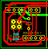
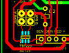
My first time using these tiny things. My soldering skills are good. Ive read that 63/37 is a good idea so i have a roll on order. i just need your input on track sizes. In my PCB ive made them as wide as the SMDs leads. Just want to know if i might run into any unforeseen issues. this s a TTP223


")

