Continue to Site

Welcome to our site!

Electro Tech is an online community (with over 170,000 members) who enjoy talking about and building electronic circuits, projects and gadgets. To participate you need to register. Registration is free. Click here to register now.

  • Welcome to our site! Electro Tech is an online community (with over 170,000 members) who enjoy talking about and building electronic circuits, projects and gadgets. To participate you need to register. Registration is free. Click here to register now.

SMD components and track size.

Status
Not open for further replies.
If you can move JumperA and JumperB up some...
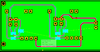
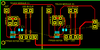
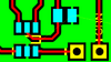
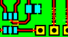
I did what you have suggested. Pic 7 is before the pour with just the ground tracks present and not routed. pic 8 is after the top n bottom pours. . You can see the tracks visible. I ran the DNC and it showed no errors. LMK if i missed anything. I have also neatened it up some. Not shown
 

Attachments

  • SMT-ADVICE7.png
    SMT-ADVICE7.png
    29.2 KB · Views: 192
  • SMT-ADVICE8.png
    SMT-ADVICE8.png
    27 KB · Views: 187
That’s the idea.

Just need to clean up all the unnecessary track bends (as in pic 7) before applying the pours, then your good to go…
 
Those thin yellow lines are air wires. They show points that should be connected (presumably in a schematic?) that have no real (i.e., copper trace) connection.

Surface mount pads can only be connected to the top copper layer. If you need to connect to the bottom layer, you must have a via, located a little distance from the pad.
Screenshot_20210619-164023_Edge.jpg
 
Those thin yellow lines are air wires.
Thank you for that. i was calling them "a trace". And a connected net "a route"
I cleaned up the PCB and since this latest tip utilizing pours i was able to route everything on top layer.
BTW Those LED-BI-COLOR routes are a pass through. they work through a separate circuit board.
 

Attachments

  • SMT-ADVICE9.png
    SMT-ADVICE9.png
    35.9 KB · Views: 187
Thank you for that. i was calling them "a trace". And a connected net "a route"
I cleaned up the PCB and since this latest tip utilizing pours i was able to route everything on top layer.
BTW Those LED-BI-COLOR routes are a pass through. they work through a separate circuit board.

Those "air wires" (i've never heard them called that....but anyway...) are disconnected nets. It indicates the pins that are disconnected from ground. Probably because the pour isn't applied yet in that photo. There shouldn't be any disconnects after you apply the copper pours. If there are, try running "Optimize nets" and see if they disappear. If they still appear, then they probably ARE disconnects and you need to fix.

Any pad that is connected to a copper pour should have a "Thermal relief pad" automatically applied. Thermal pad looks like this:

1624151388967.png


of course, the square/rectangle pads will be square/rectangle.
 
Last edited:
Any pad that is connected to a copper pour should have a "Thermal relief pad" automatically applied.
taking into consideration that the un-routed nets should not be there after the pour you can see that in my project they are still here (img10) but the thermal relief pads are present. After running"optimize nets" they went away. (img11)
 

Attachments

  • SMT-ADVICE10.png
    SMT-ADVICE10.png
    20.7 KB · Views: 187
  • SMT-ADVICE11.png
    SMT-ADVICE11.png
    22.1 KB · Views: 197
Status
Not open for further replies.

Latest threads

Back
Top