Continue to Site

Welcome to our site!

Electro Tech is an online community (with over 170,000 members) who enjoy talking about and building electronic circuits, projects and gadgets. To participate you need to register. Registration is free. Click here to register now.

  • Welcome to our site! Electro Tech is an online community (with over 170,000 members) who enjoy talking about and building electronic circuits, projects and gadgets. To participate you need to register. Registration is free. Click here to register now.

SMD board problems in Eagle.

Status
Not open for further replies.

Pommie

Well-Known Member
Most Helpful Member
I've decided to do a board completely surface mount in Eagle. The autorouter is pretty useless so I hand routed it. The problem comes when I run a DRC. Eagle reports every connection as a Stop Mask error. Does anyone know a way around this? See board below.
All the white hatched areas are the stop mask. However, I did the library for the 2 JST connectors and I didn't include any stop mask.

Any and all help appreciated.

Mike.
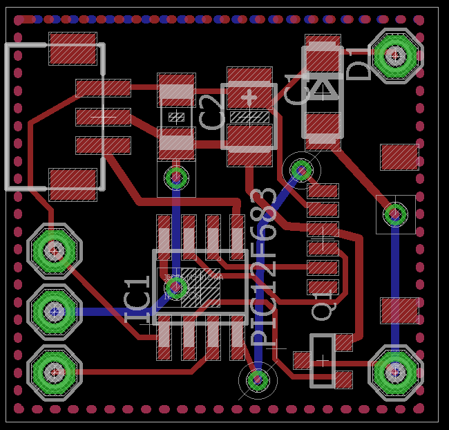
SM board.png
 
Hi Pommie.
how are you !! please send me a .brd file and let me also see the drc messages.
and if possible, sch also.
 
Here's the sch and brd files. Had to rename the sch file to txt.

Mike.
 

Attachments

  • Belt daughter.brd
    59.5 KB · Views: 231
  • Belt daughter.txt
    665.1 KB · Views: 270
BTW, I am using version 7.6 and it's not compatible with previous versions.

Mike.
 
i understand.
here i have a link to "stopmask"error and its treatment. please see if this could help you.
Incidentally I was able to open and use the files.
the vss and vdd connection can be removed and the polygons , once named , would take care pummy.
**broken link removed**

PS: **broken link removed**
this shows another member solving his issue using the suggestion.
 
in the help , under 'context' i find these comments, Pommie.
Masks
The Masks tab defines the dimensions of solder stop and cream masks. They are given in percent of the smaller dimension of smds, pads and vias and can have an absolute minimum and maximum value.
Solder stop masks are generated for smds, pads and those vias that have a drill diameter that exceeds the given Limit parameter.
Cream masks are generated for smds only.


Otherwise I am yet to resolve the issue.
 
Go to the Layer Settings on the top left and turn off the display of those layers. It will only DRC the layers that are visible. You have a lot of layers on for some reason. Just turn on the ones that you are using. Top, bottom, pads, vias, dimensions, silk...
 
I redid the board with the drc file from DirtyPCB's website and all errors disappeared. Probably because of the Stop layer being off.

Thanks all for the help.

Mike.
 
Status
Not open for further replies.

Latest threads

New Articles From Microcontroller Tips

Back
Top