Continue to Site

Welcome to our site!

Electro Tech is an online community (with over 170,000 members) who enjoy talking about and building electronic circuits, projects and gadgets. To participate you need to register. Registration is free. Click here to register now.

  • Welcome to our site! Electro Tech is an online community (with over 170,000 members) who enjoy talking about and building electronic circuits, projects and gadgets. To participate you need to register. Registration is free. Click here to register now.

Simple solar voltage clipping circuit

Status
Not open for further replies.

SimonSolar2C

New Member
Hi, I have been trying to design a low cost small circuit to voltage clip off my small 2watt solar cell's 7volt voltage when it is open circuit so my phone will charge off it.
My iPhone charges from 4 to 6.2 volts.
Solar panel is Voc=7v, Isc=280ma

Ideally the solar panel would sit at 7 volts so it doesnt produce current and when the phone connects it "sees" 6.2 volts so it starts charging, pulls the voltage down to start generating current.
I dont think a volatage regulator is required - that is sort of over engineered and I want the solution to be simple that I can build into my cable.

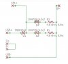
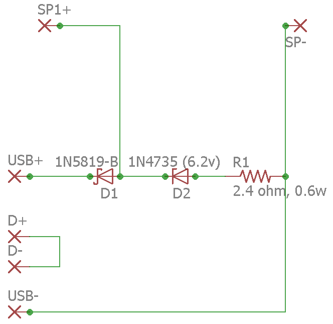
My first idea of a simple zener shunt causes too much heat in the zener.
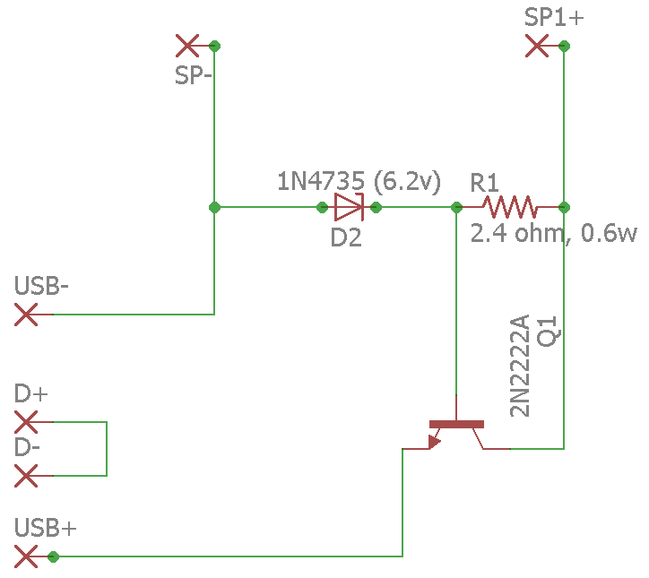
My second idea uses a transistor, but Im not sure if that is just redundant.
Any suggestions from analogue experts appreciated
0g0d2s9dymw6.png


Transistor circuit idea:
ngb9q1xy8dq1.png
 
Hi spec - thanks very much for those options.
When the current is drawn by the load, the solar panel voltage reduces. Will either of those options equalise the load to the supply when current is drawn? Ie option one will always have 2 diode drops, option two and three always have one diode drop over the transistor right?
 
Hi spec - thanks very much for those options.
No sweat SS.:) and welcome to New Zealand from the UK.
When the current is drawn by the load, the solar panel voltage reduces. Will either of those options equalize the load to the supply when current is drawn? Ie option one will always have 2 diode drops, option two and three always have one diode drop over the transistor right?
Assuming the current load is 1 mA to 280 mA:

Option 1
(1) Will always be around, 2*0.6V = 1.2V less than the solar panel voltage.
Option 2
(1) If the solar panel out put voltage is 6.5V or higher the output voltage will be 6.2V - 0.6V = 5.6V
(2) If the solar panel output voltage is less than 6.5V, the output voltage will be around 0.9V less than the solar panel voltage
Option 3
(1) If the solar panel output voltage is 7.1V or over, the output voltage will be 6.8V - (2 * 0.6V) = 5.6V.
(2) If the solar panel output voltage is less than 6.8V, the output voltage will be around 1.5V less than the solar panel output voltage.

If you want a constant 5.2V, which is an ideal voltage for a USB power line, you need a step-down/step-up (buck/boost), switch-mode, voltage regulator- they are quite small and available on the net for a song.:cool:

https://www.trademe.co.nz/electroni...ronic-components/other/auction-1227471318.htm
https://www.ebay.com/itm/DC-DC-Boos...864741?hash=item258c7e1b65:g:K-IAAOSwkl5XdjBM
https://www.ebay.com/sch/i.html?_fr...ly.TRS0&_nkw=buck+boost+power+supply&_sacat=0
https://www.ebay.com.au/sch/i.html?...r.TRS0&_nkw=USB+buck+boost+converter&_sacat=0

spec
 
Last edited:
Hi spec - thanks for explaining. And greetings to you from way down here in NZ.
Of course I prefer the version 2 with less voltage drop.
I'm trying to build this in cable so the eBay version wont work for me.
My first option, before posting here, of just having a 6.2v zener shunting across the +/- seems to meet all my requirements : (be ignored when the phone is charging so solar panel will drop down to its sweet spot Vmp, and hold the voltage low enough for phone to detect correct voltage when there is no draw.)
The only disadvantage is that the zener got too hot in the sun, trying to disapate all that power.
Are both transistors required? Why is it for necessary gain? Maybe there is a single darlington pair that would do better?
 
I'm trying to build this in cable so the eBay version wont work for me.
Shame, because technically that is the way to go. Can't you put the switch-mode converter in your solar panel and simply have a USB socket on your solar panel to plug any USB device into?

My first option, before posting here, of just having a 6.2v Zener shunting across the +/- seems to meet all my requirements : (be ignored when the phone is charging so solar panel will drop down to its sweet spot Vmp, and hold the voltage low enough for phone to detect correct voltage when there is no draw.) The only disadvantage is that the Zener got too hot in the sun, trying to dissipate all that power.
That, shunt approach uses constant power and when the phone is not plugged the Zener diode will dissipate around 2 Watts, so it will get hot and would need a heat-sink or a 3W Zener diode with a free flow of air no higher than around 5 Deg C around it- all off the top of my head that is.
Are both transistors required?
In option #2 the two transistors behave like a Darlington and in option #3 the two transistors are connected as a Darlington pair

Why is it for necessary gain?
Yes- the two transistors feeding each other have a current gain of around 1,000, compared to a single transistor gain of around 30 to 50. This reduces the quiescent dissipation in the shunt Zener diode from around 2W to around 62mW.

Maybe there is a single Darlington pair that would do better?
Darlington transistors are not that common, and are oftem more trouble than they are worth.

You can get surface mount components, so option #2 could be made very small. But note that whatever approach you use, apart from switch-mode, you will always dissipate (Vin- Vout) * I which, from what you say, could be, 2V * 280mA = 560mW, when the phone is on charge and almost nothing when the phone is not on charge.

I will see if I can come up with another approach.

spec
 
Last edited:
Hi again SS,

I have added a fourth option to the schematic in post #2 for you to consider.

spec
 
That forth option looks very interesting. Note that we dont really want any power disappated in the circuit whilst phone is charging - solar is all about efficiency;)
 
Hi Spec - just to clarify, once the phone starts drawing power, the supply voltage comes down. Right down to 5v is possible.
 
The Si8824EDB is surprisingly small. It would be great to fit this on a 5x8mm board inside the cable, but I didnt expext <1mm compionent size. We do have a bit more space available if you had a preferred alternative.
 
The Si8824EDB is surprisingly small. It would be great to fit this on a 5x8mm board inside the cable, but I didn't expect <1mm compionent size. We do have a bit more space available if you had a preferred alternative.
Yes, electronic components can be incredibly small theses days, and can fit into the smallest spaces. But fitting surface mount components can be extremely difficult, unless you are experienced and have the appropriate tools.

There are, in general, the following categories of component sizes:
(1) Tradition through hole: ideal for home makers
(2) First-generation surface mount: OK for home makers
(3) Second-generation surface mount: difficult for home makers (special optical and soldering tools required)
(4) Third-generation surface mount: impossible for home makers (extreme manual dexterity and expensive specialist tools required)
(5) Ball grid array (BGA): totally impossible for home makers (not only is the process difficult but joints cannot be inspected, so the success of BGA relies on a highly precise manufacturing control). But, low-pin-count BGA packages, transistors and opamps for example, can be mounted balls-up so that wires can be attached to the solder balls.

But, in spite of the above comments, some home makers do carry out all the above manufacturing processes, but they are exceptionally skilled and have the necessary equipment- often salvaged, re-purposed, or home-made.

In view of what you have said, I will have a look at a better approach for your USB pre-power supply.

spec
 
Last edited:
Thank you spec. That's a very interesting classifications set. I think I would aim for (2)
No probs SS.

Very wise, I always aim to suggest circuits that use category (1) and (2) components but, unfortunately, many of the new, and super, components are only available in the higher category packaging groups.

spec
 
Last edited:
So is there a more easily available part that will do the job of Si8824EDB ?
Don't worry about any components for the time being.

Right from day one, I had knocked out a proper circuit with the following characteristics:
(1) Solar panel voltage 5.2V upwards, output voltage 5.2V, with or without current load.
(2) Solar panel voltage below 5.2V, output voltage equal to solar panel output voltage with or without current load.
(3) The circuit will consume around 2mA
(4) The 5.2V output voltage can be set to whatever voltage you like (within bounds).

In case you want to do some reading up, the circuit uses:
(1) PMOSFET
(2) Operational amplifier (opamp)
(3) 2.5V precision voltage reference.

Surface mount components mean that the circuit should fit OK in your cable

I haven't posted the circuit for you to consider because of practical reasons (visitors etc).:)

spec
 
Last edited:
Last edited:
Yes, electronic components can be incredibly small theses days, and can fit into the smallest spaces. But fitting surface mount components can be extremely difficult, unless you are experienced and have the appropriate tools.

There are, in general, the following categories of component sizes:
(1) Tradition through hole: ideal for home makers
(2) First-generation surface mount: OK for home makers
(3) Second-generation surface mount: difficult for home makers (special optical and soldering tools required)
(4) Third-generation surface mount: impossible for home makers (extreme manual dexterity and expensive specialist tools required)
(5) Ball grid array (BGA): totally impossible for home makers (not only is the process difficult but joints cannot be inspected, so the success of BGA relies on a highly precise manufacturing control). But, low-pin-count BGA packages, transistors and opamps for example, can be mounted balls-up so that wires can be attached to the solder balls.

But, in spite of the above comments, some home makers do carry out all the above manufacturing processes, but they are exceptionally skilled and have the necessary equipment- often salvaged, re-purposed, or home-made.

In view of what you have said, I will have a look at a better approach for your USB pre-power supply.

spec

I would add that because of the difficulties, various
Yes, electronic components can be incredibly small theses days, and can fit into the smallest spaces. But fitting surface mount components can be extremely difficult, unless you are experienced and have the appropriate tools.

There are, in general, the following categories of component sizes:
(1) Tradition through hole: ideal for home makers
(2) First-generation surface mount: OK for home makers
(3) Second-generation surface mount: difficult for home makers (special optical and soldering tools required)
(4) Third-generation surface mount: impossible for home makers (extreme manual dexterity and expensive specialist tools required)
(5) Ball grid array (BGA): totally impossible for home makers (not only is the process difficult but joints cannot be inspected, so the success of BGA relies on a highly precise manufacturing control). But, low-pin-count BGA packages, transistors and opamps for example, can be mounted balls-up so that wires can be attached to the solder balls.

But, in spite of the above comments, some home makers do carry out all the above manufacturing processes, but they are exceptionally skilled and have the necessary equipment- often salvaged, re-purposed, or home-made.

In view of what you have said, I will have a look at a better approach for your USB pre-power supply.

spec

I would add that because of the difficulties, various companies supply break-out boards, which are small circuit boards that take one main component, and sometimes a few auxiliary components, and provide reasonable size connections.

Here is an example:-
https://www.sparkfun.com/products/13963https://www.sparkfun.com/products/13963

Yes, those break-out boards are dead handy and can solve the problem of doing development work with components that are only available in surface mount, like the 'perfect' opamp, the OPA192 which is now my go-to opamp.

Of course, for the final implementation the OP needs the small size of surface mount components so that the voltage regulator of post #16 can be fitted in a cable.

spec
 
Last edited:
Hi -I like your elegant solution with opamp, thank you again Spec.
However it has left me more confused now to decide on best solution for our for our 'simple clipping circuit'
Would you think the simplest circuit a failure if I used it.
That is two 6.2v zener diodes in parallel with 4.8ohm resistors, and a schottky diode?
 

Attachments

  • v8.jpg
    v8.jpg
    15.6 KB · Views: 333
Hi -I like your elegant solution with opamp, thank you again Spec.
However it has left me more confused now to decide on best solution for our for our 'simple clipping circuit'
Would you think the simplest circuit a failure if I used it.
That is two 6.2v zener diodes in parallel with 4.8ohm resistors, and a schottky diode?
Hi SS,

If the circuit that you want to use does the job, then go for it.:)

spec
 
Status
Not open for further replies.

Latest threads

New Articles From Microcontroller Tips

Back
Top