Continue to Site

Welcome to our site!

Electro Tech is an online community (with over 170,000 members) who enjoy talking about and building electronic circuits, projects and gadgets. To participate you need to register. Registration is free. Click here to register now.

  • Welcome to our site! Electro Tech is an online community (with over 170,000 members) who enjoy talking about and building electronic circuits, projects and gadgets. To participate you need to register. Registration is free. Click here to register now.

Simple DC-DC converter

Status
Not open for further replies.

Steam

New Member
Hello!

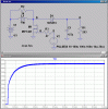
I need to make simple boost converter. 4.5V Input and 45V output. I need only about 10W output. Here is circuit:
**broken link removed**
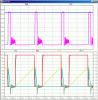
I have clock source with duty cycle = 0.9
I don't know how to calculate L1, R1 and C1.
R2 is load and I choosed 203 Ohms (U=45V, P=10W then R=202.5).

It's not necessary to have 45V output, output can vary +-10V.

Can somebody help me? Excuse me for my bad english.
 
Ok, i've found some formulas, but I don't understand from where did they came from.
L(min) = D*Vin*(1-D)/(2F*Iout)
Ipeak=(Vin*D)/(F*L)
Cmin=Iout/F/Vripple
 
It is not as simple as you think!

1. The peak inductor current requirement is large. You will have a hard time to find a commercial inductor which supports ~6A without core saturation. Can your battery supply a peak current of 6A?

2. C1 must be much larger to filter the pulses, even though I raised the switching frequency to 50Khz. Note the gate drive duty cycle to get ~45V out.

3. The NFET drive requirements are critical: Gate Driver impedance MUST be very low (see the 47Ω (R3), otherwise the gate capacitance will slow the rise/fall time of the gate signal, slowing the FET switching times, causing HUGE dissipation in the FET. The amplitude of the gate drive must be sufficient to saturate the FET. Typical gate drive level is 10V. Logic-level FET might allow 5V gate drive; 4.5V will be marginal.

4. The power dissipation of the NFET is ~2W, so it will have to be heatsinked.
 

Attachments

  • Boost1.gif
    Boost1.gif
    56.2 KB · Views: 1,900
  • Boost2.gif
    Boost2.gif
    34.7 KB · Views: 1,211
Last edited:
Thank you!

So what max current I can have at 45V if I'm going to use hand-made air-core inductor?
 
You will never get what you need with an air-core inductor. There are commercial inductors that can handle that amperage; I know digi-key sells some. I just bought some 24A inductors from them. At 10W that's only about 600ma output, so only about 6A input, with a peak of ~8.2A or so.

4.5 to 45v might be too much for a single stage boost. You might have to make it a double stage. This would also limit your peak currents through the inductors as well, reducing their requirements.

Is this a constant load? Boost converters without any feedback regulation require a load that never changes, otherwise they will blow themselves up.
 
Last edited:
smanches said:
You will never get what you need with an air-core inductor.
So what max can I get from air-core inductor? 0.1W possible?

smanches said:
4.5 to 45v might be too much for a single stage boost. You might have to make it a double stage. This would also limit your peak currents through the inductors as well, reducing their requirements.
That's a good idea! Thank you!

smanches said:
Is this a constant load?
No. I need this converter to charge 10 000 uF capacitor.

Sorry I'm bad in this section, I have only some experience working with microcontrollers, but none with analogue technics
 
There is a circuit here that only needs 2 transistors, it operates at a constant INPUT current (ie average inductor current) so it fixes some of the problems with boost converters and max current in the inductor etc, see here;
+5v to +12v converter

It's perfect for charging a cap due to the regulated input current. However I don't know how well it will work if you need real fast charging. It is ok for smaller wattage like 1A at 4.5v input.
 
Mr RB, thank you for the schematics.

Ok, I've tryed to analyse this thing:
**broken link removed**
R2 is equivalent to B1 internal impedance.
The top graphic is current form 18 to 20 secunds. Bottom - from 0 to 20 secunds voltage on the capacitor.
Using Proteus.
As you can see this thing is working good, and (If I'm not wrong) going to make simple feedback: when voltage reaches (for example) 70V, then just turning off Q1.
In this schematic I used 9V pulse voltage source with D=0.9 (to the Q1 gate). So I think about this kind of feedback: simple use voltage divider by factor 20 and then compare it with zener voltage and if voltage on divider is higher, then stop oscillator.

And last question: what inductor do I need? how to calculate?
 
Last edited:
The bigger the inductor, the lower the gate frequency which will keep the inductor current within reason.

In your simulation, you need to account for a real load. Add a load resistor in parallel with the output capacitor. Look at my sim again.
 
Before I start let me say that I work at Maxim. May I suggest using a DC-DC controller IC? Most companies will give a free sample, so cost shouldn't be an issue. A part like the MAX668 will do this pretty easily (as will parts from other companies) and there are equations on the data sheet that will help you pick component values. With a chip, you get a nice fixed operating frequency so it's easier to pick component values, and a regulation loop so your output voltage stays put with load variations. What you've drawn so far risks soaring at no load and blowing your output caps. Also, to contradict one other comment, you should have no problem doing a 10x voltage boost with one boost stage.
 
Thank you for suggestions!

I'm just trying to simplify circuit as much as possible. I live in Russia, so we don't have any companies that will give me a free sample of DC-DC controller IC (and it tooks a lot of time to ship something from europe or USA, or even from Moscow).

So, here is another circuit:
**broken link removed**

U1 is 555 timer. It's set in astable mode with D something around 0.9. D1-Q3 is "detector" if voltage from "5+5sin(t)" is higher than Zener's voltage. Q4 is signal inverter from Q3 (like logical NOT). Q1 is "swithcing" off and on the voltage booster. Q2 is part of the booster (switcher). R5 is inductor's resistance equivalent.

I set up such low freq just to demonstrate circuit work.

You can see diagram. There are two curves: Red is "5+5sin(t)" and Green (5*Current).

The way the circuit works:
If we have voltage on D1 lower than some value, than we've got signal with D ~0.9 and capacitor (outside this scheme) is charging. When voltage from capacitor reaches some value (D1*voltage_divider_factor), then booster's "switch" is going to be off. and when capacitor's voltage will be lower then (D1*voltage_divider_factor) we again have signal with D~0.9.

According to the simulation results the circuit is runing good. This is not the full circuit! another components of the booster need to be added! This is just some kind of feedback circuit.

Have a good day.
 
Last edited:
Status
Not open for further replies.

Latest threads

New Articles From Microcontroller Tips

Back
Top