Continue to Site

Welcome to our site!

Electro Tech is an online community (with over 170,000 members) who enjoy talking about and building electronic circuits, projects and gadgets. To participate you need to register. Registration is free. Click here to register now.

  • Welcome to our site! Electro Tech is an online community (with over 170,000 members) who enjoy talking about and building electronic circuits, projects and gadgets. To participate you need to register. Registration is free. Click here to register now.

Si826x gate driver keeps failing

Status
Not open for further replies.
Hi,
I'm having a problem with an isolated half bridge driver circuit where the gate driver keeps failing.

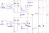
I'm trying to use two "Si8261BBC-C-IP" isolated gate driver ICs to isolate the MCU from the MOSFETs, but the driver keeps failing after less than 1 minute. As soon as I replace the component with a "FOD3180TV", the circuit works for more than one hour. The MOSFETs however are fine as well as the MCU. It's just the gate drivers that keeps on failing, especially the low side driver.

At this stage I'm only building a test circuit which is running at about 50-kHz and a 40 % duty cycle and a resistor as a "load".

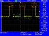
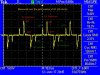
I would really like to have someone just look at my circuit diagram and make a suggestion as to what might be wrong or what I might improve on. The problem is that the gate driver keeps failing and I just simply cannot understand why and what is wrong. The output of the circuit (as measured on an oscilloscope) seems to be a perfect square wave.

Any advice would be greatly appreciated.

Kind Regards
 

Attachments

  • Isolated_Phase_Shifted_Half_Bridge.pdf
    59.4 KB · Views: 109
  • test.jpg
    test.jpg
    186.2 KB · Views: 154
Si8261 I have used many and never had a failure.
Your boot strap diode is 4A. I use a 1A part. Not a real problem. Just a comment.
I put a 0.1uF cap in the driver supply pins.
Do you have some dead time? If you turn on Q1 at the same time as you turn off Q2 there will be a short time when both MOSFETs are on. Maybe only 20nS. This causes very large currents that you might not see. You should have 100nS of dead time where neither MOSFET is on. These very large currents will cause spikes that kill silicon.
What is the layout like? PCB? Point to point wires? I place the driver very close to the Gate. I think you may have inductance from long wire. This will cause spikes. What is the distance from IC to MOSFET?
---edited----
Your "28" volt protection on the gate of the MOSFETs actually clamps at 31 to 34 volts. So the protection is not doing anything. (MOSFET G-S voltage must be below 30V)
 
Last edited:
Hi, thanks for the reply.

The part number for the actual MOSFETs that I'm using is IXTH48N65X2 and the actual values for the TVS diodes on the gate-source is P6KE24CA. I just used the closest values that I could find in Multisim as I couldn't find the exact part numbers. The PCB traces are on a vero / prototyping board, the driver is about 18mm max from the MOSFET gate pin. The dead time is quite long, for now I'm using a T494 PWM chip to mimic my MCU that I want to use. Since my duty cycle is 40%, the actual time in seconds should be 200 microseconds. I haven't measured the voltage across the 20-ohm resistor, but I think that should give me some idea of how much current is flowing?

I'll measure that some time this week using a LeCroy Waverunner, but I don't understand why the FOD3180 don't seem to fail. I must be missing something.

It also seems that when I increase the voltage from 24V to something like 30V, they fail even quicker. Note that the power supply that supply the gate driver and the power supply that's connected to the MOSFETs are two different power supplies with two different grounds. The gate driver supply is always 15V, but whenever I increase the voltage of the half bridge, the driver fails instantly. I don't know if it has something to do with MOSFET capacitances?
 

Attachments

  • Trace.jpg
    Trace.jpg
    107.7 KB · Views: 125
Does the IC get hot before it dies? warm?

With the 15V on and the 24V off; does the IC die?
With the 15V on and the 24V on and R_load removed: does the IC die?
Just trying to understand when the IC dies.

On the TL494; are you using one output to drive Q1 and the other output to drive Q2?
OR
On the TL494; are the two outputs tied together? A low turns on Q1 and a high turns on Q2?
 
Nope, doesn't get hot before it dies. It does however get hot the moment it dies because the output mosfets inside the driver gets shorted together.

With the 15V on and the 24V off, the gate drivers never fail.
With the 15V on and the 24V on, with or without load the chip dies. If there is no load however, in other words no minimum load, the driver dies immediately. I assume this would be because the Drain-Source capacitance inside the mosfet doesn't discharge in time.

On the TL494, each output drives Q1 and Q2 separately.
 
On the TL494, each output drives Q1 and Q2 separately.
There is no crossover problem. Good.
I think the way you have it:
Q1 = on Q2 = off
Q1 = off Q2= off
Q1 = off Q2 = on
Q1 = off Q2 = off
With the 15V on and the 24V off, the gate drivers never fail.
Good. So the LED side of things is not failing. (input)
If there is no load however, in other words no minimum load, the driver dies immediately. I assume this would be because the Drain-Source capacitance inside the mosfet doesn't discharge in time.
I am sure there is a clue there. With load it dies with some time. With no load it dies immediately.
I think the D-S capacitance is not a problem. 20 ohms on the gate limits the current. Often I run more like 4.7 ohms.

One would think that if too much current (heat) killed the part, then a finger on the IC should show a heat problem.
I still think "inductive kick back" from long wires (over voltage) is likely but your layout looks good. (can not see it all) alec_t sent good information.

The IC is good for 30V and you are running 15 so DC voltage is good.
 
I must agree with ronsimpson about the need for a 0.1uF cap close to the power supply pins of each driver. You show a 1uF and a 10uF cap, but they're shown as polarized parts, so I assume that they're electrolytics

While lower in capacitance, the low equivalent series resistance, impedance and inductance characteristics of ceramic capacitors do things that their higher value electrolytic and tantalum cousins just can't.

And, although we usually think of them as decoupling caps to supply supply spikes of current when a change of state in a chip increases it's demand, they also do a great job at stabilizing the supply rails against voltage spikes due to transients in other parts of the circuit.
 
impedance and inductance characteristics of ceramic capacitors do things that their higher value electrolytic and tantalum cousins just can't.
The IC can pull down with 0.8 ohms and up with 2.6 ohms.
I just looked up the ESR (internal resistance) of 1uf 50 to 63V ele. caps. Digikey.com shows 3 to 30 ohms depending in case size and cost. I looked up the king I am using and they are 12 ohm. (good parts)
Digikey shows that most 10uF 50-63V ele caps have a resistance of 1 to 10 ohms.
I did not look for inductance.
I looked up muRata ceramic capacitors. The resistance depends on case size. Runs 0.1 to 1 ohm.

If the IC is being killed by inductive kickback, a low resistance, low inductance capacitor across the power supply pins of the IC will help. Keep lead length short. (think about your capacitors having 10 ohms inside) or 0.1 to 1 ohm for a ceramic 1uF.
 
I did some further testing. I added a load to the half bridge stage and saw that when no minimum load is present, the gate drivers will fail immediately. With a minimum load drawing at least 0.5 A, they don't fail anymore.

Just other things I do note. This board is just a prototype or rather a prototype of a prototype. In the past I've always used gate drive transformers or a regular gate driver IC like IR2110, this is just something new I wanted to try instead as it can simplify and shrink the circuit significantly. So yes, I agree that a 0.1uF cap is needed, but I don't think this is the primary cause for them failing. For final stage implementation - Yes, I will certainly add them, for a prototype - NO. I will explain this just now.

I tested the Vcc-GND voltage across each driver (High and Low Side) on the scope. There was no detectable ripple at all. If the omission of the 0.1uF cap or the electrolytic caps having a high ESR and inductance was the cause, then I would've seen some voltage spikes, however I saw zilch. Second reason is that the driver output stage always seemed to NOT be shorted across Vcc-to-GND but rather between Vout-to-Vcc or Vout-to-GND. This tells me there are spikes coming from the MOSFET gate causing the schmitt-trigger FETs to fail.

I measured the voltage across the 20-ohm resistor and I saw some very high spikes when I remove the load of the half bridge. This decreased when I increased the load. Peaks reached about 9-10V over the 20-ohm resistor, indicating about 0.5A peaks. The driver states that it can handle 4A peaks.

Last thing I noticed. I did a torture test on the two drivers. One is FOD3180 (2A peaks) and the other SI8261BBC (4A peaks). I found something very, very interesting. I added random caps in increasing numbers and sure enough, the FOD3180 could handle spikes of up to 2A (remember I'm talking about peak spikes of very, very short duration). Over that and it would fail. However, the SI8261BBC barely managed over 0.9A (peak) before it fails. I don't get it as to why since they're supposed to be stronger.

However something else I'm seeing is that When the low side FET is switching, it's highly detectable on the gate of Q1, causing about 200-250mA to be sink/sourced by its driver, which must not be the case. The opposite is also true. I haven't got the time yet to figure all of that out yet, I'll read through the whole PDF that Alec_t posted sometime tomorrow.

In the 1st image, this was measured on the PWM generator for Q1 (just to show when what switches and the dead time). Then the 2nd image shows the voltage over Q2. It doesn't matter whether its high or low side, they both look the same. I'm assuming this can cause me potential further problems. I'll probably look into it in the coming week.
 

Attachments

  • 1.jpg
    1.jpg
    177.3 KB · Views: 130
  • 2.jpg
    2.jpg
    199.7 KB · Views: 115
Status
Not open for further replies.

Latest threads

New Articles From Microcontroller Tips

Back
Top