Continue to Site

Welcome to our site!

Electro Tech is an online community (with over 170,000 members) who enjoy talking about and building electronic circuits, projects and gadgets. To participate you need to register. Registration is free. Click here to register now.

  • Welcome to our site! Electro Tech is an online community (with over 170,000 members) who enjoy talking about and building electronic circuits, projects and gadgets. To participate you need to register. Registration is free. Click here to register now.

See any mistakes with this circuit design?

Status
Not open for further replies.

ACharnley

Member
It's a load based darlington shunt with a mosfet stage for greater efficiency. The zener values will need adjusting so that the stages sync.

The source is low impedance; it will drop significantly under load. Normally the darlington stage won't be used but when it needs to shunt some of the power it is load based, rather than a straight zener clamp.

Am I missing anything?

PS) transistor on right is also darlington.
 

Attachments

  • DSC_0267.JPG
    DSC_0267.JPG
    563.3 KB · Views: 165
  • DSC_0267.JPG
    DSC_0267.JPG
    563.3 KB · Views: 158
Silly me, there'd be a resistor instead of a link right of the top mosfet protection diode connection.

Also the drain resistor probably isn't needed.
 
Last edited:
The way the schematic is drawn, the darlington transistor will saturate whenever the input is above 2 V, putting the full input voltage across the load. Nothing to the right will matter.

I have no idea what an "efficient opto" is.

If you want to clamp the FET Vgs to something under 20 V (the usual datasheet max.), there is no advantage to having a transistor and zener in parallel with another zener.

Keep the gate-source resistor; it improves turn-off times and helps protect the gate from ESD damage.

Redraw the schematic with reference designators and values/part numbers for all components.

In terms of input voltage conditions and load conditions, what is the purpose of the circuit?

Where are you located?

ak
 
The darlington has a 1.4v drop (approx) while the mosfet has virtually none.

I should add that the load operates at >5v, nominal load voltage is about 8v and efficiency during operation is everything (1.4v is quite a % at 8v).

The FET will "short the darlington" up to 24v (approx, but 25v is the limit). This is why there's the second zener to handle the max mosfet vgs (and missing resistor I mentioned).

I'm not at the point of selecting components/values, it's just to test the logic.
 
Last edited:
The darlington has a 1.4v drop (approx) while the mosfet has virtually none.
Are you stating the 1.4 V drop as the saturation voltage Vcesat, or the combined base-emitter voltage? If the latter, then your comparison to a FET is incorrect.

What is the max. load current? That will help determine the voltage drop across the FET.

ak
 
I'm not comparing it to a FET. The 1.2-1.4v is the base-emitter voltage drop. The voltage drop of the FET is inconsequential, the load will only work at 5v+ and at that point a low vgs FET will have minimal voltage drop.

Here is a table of expected input voltage vs load voltage with this design:

Input V, Load V
0 , 0
1, 0
2, 0.8
3, 1.8
4, 2.8
5, 4.9
6, 6,
7 - 23, 7 - 23
>24, 23
 
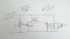
So at 100 V input, there will be 23 V across the load and77 V across the transistors? At any load current above 25 mA you will need heatsinks and possibly a fan.

Back to the voltage "drop"...
(1.4v is quite a % at 8v).
That would matter if that 1.4 V were in series with the load, but it is not. The *saturation voltage* Vcesat (not Vbe) is in series with the load, and by definition that is lower than Vbe. The only "efficiency" difference between a MOSFET and a BJT is the gate energy versus the base-emitter energy. A power MOSFET typically has a higher gate voltage for full enhancement than a BJT base-emitter voltage does for saturation, but the steady-state gate current is so much less than the base current that the total energy is less. But even a logic level MOSFET needs over 2 V for full enhancement, while you state that the BJT needs only 1.4 V for saturation.

Efficiency is the output power divided by the total circuit power. At its heart, the circuit is a linear regulator, so by definition it is the least efficient power regulator topology possible, equivalent to using relays to switch resistors in series with the load. No matter how many power devices share the load current, the efficiency is the same. Since the load current is a secret, let's assume 1 A. At 100 Vdc input, there is 23 W dissipated in the (secret) load and 77 W dissipated in the regulator. This is almost completely independent of the number or types of regulator pass devices. Almost, because (not counting the current through the various zeners) if the only pass element is a power darlington, its base current is something less than 1 mA while the gate current of an equivalent MOSFET will be under 1 uA. That is a thousand-to-one difference, but in something that is very small to begin with. The base current is less than 0.1% of the total circuit current, so it is a barely measurable effect on efficiency.

What I *think* you are trying to say is that a fully "on" power MOSFET has a lower Vds voltage drop in series with your load than would a fully saturated BJT Vce. That usually is true; but not always, depending on the rest of the circuit parameters and the specific components chosen. To have the BJT conduct only when the input is above 24 V, put a 22 V zener in series with the base. This increases the transistor's effective "turn on voltage" to 23.4 V. Note that typical zener diodes are only 5% or 10% accurate, the zener voltage changes with its series current, and the BJT base-emitter conduction voltage also changes with both base and collector current.

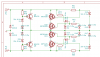
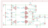
A final note, many power darlington transistors have two base-emitter resistors built-in. These need to be a part of the overall circuit efficiency calculation.

Based on the information you have released so far, sharing the load current between two power devices is not necessary, and decreases both the overall circuit reliability and its "efficiency".

Also, I think what you are trying to build is a 23 V voltage regulator that has a very low series voltage drop when the input is less than 23 V. This is called an LDO (Low Drop Out) circuit. There are many examples on the internet, and control chips for this specific purpose if you don't want to grow the circuit from scratch.

What is the peak load current?

ak
 
Last edited:
The "load" is a buck regulator, the mosfet is to ensure maximum efficiency under normal operation and the darlington is the main protection.

The Vcssat is typically similar to Vbe or at least it's enough to cause an efficiency drop. Efficiency at the norminal Vin of 7-8V is critical.

I haven't calculated the zeners, they'll have to be matched with the darlingtons to ensure sync. Too early a stage for it.

Current is 500mA. 100V is realistically not going to occur but is to allow headroom for a brief spike, 60V is a more accurate maximum over, potentially 60 seconds. That sort of wattage isn't possible, a large load will cause a significant voltage drop at Vin, the maximum Vin voltage is for no load, in which case there'll be no heat dissipation through the darlington. That's the benefit over using large parallel Zeners - it's just the efficiency drop during normal operation that I wished to target.
 
My apologies, the darlington has a 0.9v drop (getting mixed up there).

This is what I've come up. The top half of the circuit would mirror and connect to the + rail, the FETS now form a semi-active rectifier. The disadvantage is the skhottkys will need to be silicon to withstand the potential 100VAC. The FET's will have to have a gate-source breakdown of 100V as well, which potentially limits to a higher Rds upto 0.5ohm for the pair.

What I'm left with then is 0.7v (silicon) + 0.5ohm) during normal operation, 0.9V+0.7V + shunt at higher voltages (when efficiency doesn't matter), plus heat generated is still based on the load - no load, no heat.

The alternative to all this is a pair of zener's to shunt the voltage (potentially a lot of heat, not load based) and a bridge skhottky, around 0.6v drop.

I believe the benefits are worth pursuing.
 

Attachments

  • DSC_0273.JPG
    DSC_0273.JPG
    528.4 KB · Views: 143
In your posts #1, 2, 4, 6, and 8, the input was DC. Is it now AC?

ak
 
Yeah, at first I had the rectification done beforehand, but duplicating the circuit allows for the mosfet's to be used for AC semi-active rectification.

I'm wondering;

a) if I can clean up those dual n-mosfet's with a p-mosfet.
b) if the reverse diode blocker to the right of the fets, which will only allow discharge to 0.7v, would still allow sufficient current to reverse flow through them when the AC reverses.

Regards, Andrew
 
Last edited:
I'm creating a schematic, but I spotted a problem - I didn't realise most darlington's have a protection diode, which will get in the way of using them for AC regulation. I'm wondering if a normal NPN like a BD139 will have enough gain to be reliable enough.
 
Those I can find yes. I'm finding plenty of darlington DC regulator examples but not for AC (could be the reason). A transistor will likely work, even if I have to turn on the regulation much earlier, say 15V it is still well above the nominal voltage. Will keep looking.

I've included a N-channel to reverse block (Q9/Q12) and P-channel to turn off once voltage rises above the threshold.

The zener values need adjusting but the idea is the FETS shut off just before the transistor begins shunting.

What I've come up with so far is attached.

Error: Z10, Z13 should be inverted.
 

Attachments

  • Screenshot from 2017-06-05 12-41-33.png
    Screenshot from 2017-06-05 12-41-33.png
    34 KB · Views: 103
Last edited:
System parameters:

AC: 0-100V , 500mA fixed
Nominal operational voltage - 5.5v - 25v

Requirements:

Highest rectification efficiency during nominal voltage range (5.5- 25~v, which will then drive a buck). The buck outputs 5V so low voltage dropout is critical.
Load based (series) regulation for higher voltage range - no power disconnect. Efficiency is less important here since a higher AC voltage generally indicates no or little load is attached (so the series loss will be minimal anyway).

Considered:

Zener clamp - creates too much heat when no load is attached and over-voltage occurs.
100V buck - none operate at the full nominal voltage range
Ideal bridge - as per Buck, 9v seems minimal
Semi-active bridge (doesn't require syncing of 4x fets) is now integrated into this design. The bad news is without placing them after a zener clamp the skhottys must withstand 100v and generally this means a 0.6v drop. I have this voltage drop level already via a schkotty full wave bridge and it works fine, so 0.6v is acceptable.
 
I've changed the circuit (the top half only) to use a depletion n-channel which simplifies matters.
 

Attachments

  • Screenshot from 2017-06-05 14-20-34.png
    Screenshot from 2017-06-05 14-20-34.png
    31.7 KB · Views: 115
I'm finding plenty of darlington DC regulator examples but not for AC (could be the reason).
Nope. The reason is that using a regulator pass device as the rectifier just isn't done. Besides subjecting the regulator control circuit to large reverse voltages, it is the wrong part for the job. Rectification is on-off switching. Linear regulation is exactly *not* that.

First, can the system run with half-wave rectification as in the earlier posts, or do you need full-wave? Either way, it sounds like what you need is an active rectifier, sometimes called a perfect diode or ideal diode circuit.

https://www.linear.com/parametric/powerpath_controllers_*_ideal_diodes

ak
 
Full wave. Active rectifiers like the one you linked to only begin at 9V. It doesn't solve the higher voltage either - any buck that can do 100V will also begin at around the 8V mark, and offer less current and efficiency.
 
There are some contradictory targets in your posts so far. (unless I'm mis-reading something)
- High efficiency.
- Shunt regulator.
Generally speaking, a shunt regulator is the least efficient regulator type.

May I ask what your overall operational spec is?
- Input voltage range? AC? DC?
- Output voltage and current requirement?
 
Not really Chris, I'm trying to have my cake and eat it. :)

The shunt is the most efficient until it is active, then it is the worst. My attempt is to use a series regulator with a FET bypass within the buck voltage range. I've attempted to duplicate to handle both sides of the wave, the idea being to save a few perilous milivolts. The disadvantage of regulating after rectification is the need for a 100V bridge. Skhotties of this voltage have a 0.6v voltage drop. 1.2v drop at 6V is too great an efficiency loss.

Input: AC only, range 6 - 100V, 500mA fixed.
Output, 5V, 3A.
High Efficiency Buck (96%) voltage range: 5.5 - 23v

Priorities are: voltage dropout when AC < 10V (especially 6V), efficiency under no load
 
Status
Not open for further replies.

Latest threads

New Articles From Microcontroller Tips

Back
Top