strokedmaro
New Member
couple of questions I hope you experts can help with ")
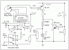
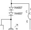
1. Attached is a piece of a schematic....Ive seen dual diodes like this in several schematics but have no idea why you would want that. can someone explain?
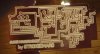
2. Ive finished etching out a PCB for my latest project but I had a thought while laying in bed last night....is there a formula to know how much current can flow through a copper trace before it fails? The trace in question is 1mm wide, 1/2 oz copper which needs to carry approx 1 amp at 12vdc. Just doesn't sound reliable to me.
THANKS!!!
1. Attached is a piece of a schematic....Ive seen dual diodes like this in several schematics but have no idea why you would want that. can someone explain?
2. Ive finished etching out a PCB for my latest project but I had a thought while laying in bed last night....is there a formula to know how much current can flow through a copper trace before it fails? The trace in question is 1mm wide, 1/2 oz copper which needs to carry approx 1 amp at 12vdc. Just doesn't sound reliable to me.
THANKS!!!
")