Continue to Site

Welcome to our site!

Electro Tech is an online community (with over 170,000 members) who enjoy talking about and building electronic circuits, projects and gadgets. To participate you need to register. Registration is free. Click here to register now.

  • Welcome to our site! Electro Tech is an online community (with over 170,000 members) who enjoy talking about and building electronic circuits, projects and gadgets. To participate you need to register. Registration is free. Click here to register now.

RF choke in power amplifiers

Status
Not open for further replies.

hanhan

Member
Hi,
Sorry for asking this question again. I really got stuck.
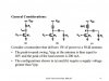
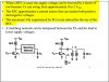
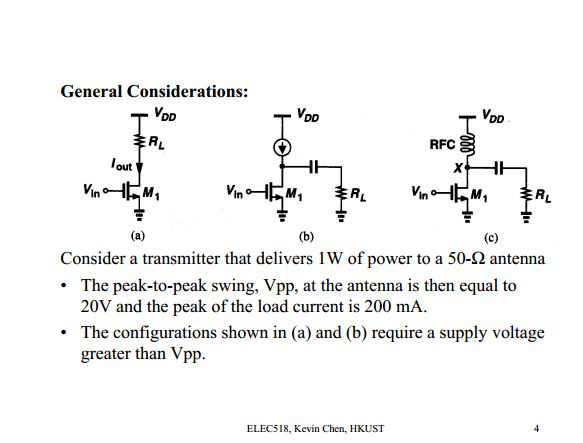
Here are two pages from this lecture slide about power amplifier: https://course.ee.ust.hk/elec518/lect11.pdf

rfc1-jpg.75202

rfc2-jpg.75203


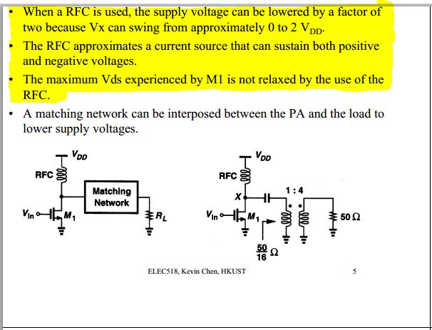
Q1: I know that Vx can swing from 0 to 2VDD but why this can be used to lower supply voltage by a factor of two?

Q2: The RFC approximates a current source. Yes, but what does they mean in "The RFC approximates a current source that can sustain both positive and negative voltages."

Q3:please help me understand this "The maximum Vds experienced by M1 is not relaxed by the use of the RFC."

Thank you.
 

Attachments

  • RFC1.JPG
    RFC1.JPG
    40.5 KB · Views: 1,200
  • RFC2.JPG
    RFC2.JPG
    57.1 KB · Views: 1,007
The text is a bit confusing. You need to go back to load lines and graphical design to see it easily.
The load on the transistor is 50 ohm. This 50 ohm gives the 'LOAD LINE' for the device. If you draw the 'collector characteristic', and then, on this graph you plot the load line for 50 ohms, you get a slope which crosses the 'VOLTS' axis at Ic= 0ma, Vc=Vdd. The other point is at Vc=0 volt, and Ic = Vdd/R. The operating curve is between Vc =0 and Vc=Vdd. The bias point for the transistor is at 1/2 Vdd so that the swing is from 0 volt to Vdd. The voltage across the load is Vdd peak to peak.
If you then use an RFC instead of the resistor load, the DC load line is a vertical line(parallel to the current axis) from Vdd ie the RFC has (theoretically) zero ohms resistance. If you now plot the 50 ohm load line from the quiescent point Vc=Vdd; Ic =200 mA, then the load line slope of the load reaches Ic=0 at a Vc of 2Vdd. So, the voltage swing available for (a) is half that for (b). Note that in (b), you need to keep the DC current out of the load by using a capacitor.
The statement "The RFC approximates a current source that can sustain both positive and negative voltages (WITH RESPECT TO Vdd)
In the case of the RFC design, the transistor can supply the load with 4 watts. In the drawing 5 of ELEC 518, the use of the coupling transformer adjusts the power dissipated in the load and allows Vdd to be set to the required value. Many of the comments need to be considered with regard to the whole text.
 
Status
Not open for further replies.

Latest threads

New Articles From Microcontroller Tips

Back
Top