Continue to Site

Welcome to our site!

Electro Tech is an online community (with over 170,000 members) who enjoy talking about and building electronic circuits, projects and gadgets. To participate you need to register. Registration is free. Click here to register now.

  • Welcome to our site! Electro Tech is an online community (with over 170,000 members) who enjoy talking about and building electronic circuits, projects and gadgets. To participate you need to register. Registration is free. Click here to register now.

Relay against load dump ?

kellogs

Member
It is pretty hard to cover all the nastiness from ISO 16750-2-2010E, and especially so when replacing a blown fuse is not desirable.

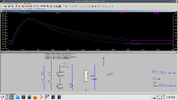
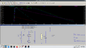
How about this approach ?

The relay armature will take some 5-ish ms to operate, which is less than the 24.4V TVS clamp can take.

I think some extra resistance will be needed ("possibly R") because i would like to use an automotive relay and these are rated for 12-16V, not 24.4V. I do want to drive it hard for a fast changeover; this relay will not have to operate more than maybe 10 times during the lifetime of a vehicle, so if it can take all those 24.4V I would not worry about # of cycles reduction.

Q1 will be operated by a MCU which interrupts on a threshold rising voltage, fast enough for the whole thing to cut off in much less than 10 ms and so the TVS clamp survives. When the surge disappears the MCU will eventually command Q1 again and operation is reestablished.

I expect this to work for a few years, but does it stand any chance to still work in 10 - 15 years ? Of course, the relay will spend 99.9999% of its life in its NC position. I wonder if an automotive relay will still be able to break the circuit after such a long time during which it has not clicked once.

load-dum-relayed.png
 
On the modelling, you really shouldn't expect the models to be correct for the various secondary characteristics of components. On a zener, the model will get the voltage correct, but I really doubt that it would model any response time, or capacitance and how that changes with voltage.
 
From a long ago time i remember simple rule "TVS fast, Zener slow".
That just means that a TVS is designed to absorb transients, while a zener is designed to run continually.

It is about the energy ratings of the TVS. A TVS is rated to absorb a certain amount of energy, while a zener is rated to dissipate a certain power, and may be more accurate in its voltage specification.

If you are trying to absorb a load dump, a lot of energy will end up in the TVS and so it will get hot during the transient and it will be difficult to know if a zener will handle that, because energy ratings are not in zener specifications.

Similarly, if you use a TVS to regulate the voltage, it may not be very accurate, and it may not be designed for continuous power dissipation, so it will just not work as well as a zener.

The load dump won't be particularly fast compared to electronic switching times, so I don't think that the switching times really come into your simulations.
 
Figures 29 - 31 shows some capacitive spikes that my simulator would not show no matter what...
The OnSemi document highlights the fact that the capacitance of the zener can cause issues of the zener voltage not changing as fast as expected.

In the circuit in post #19, the voltage across R1 would be subjected to a small spike due to the zener diode capacitance, and I think that is what you saw.
 
Just what is going on here? i was expecting for Q1's Source pin to stay at 0V until Q1's Drain pin reaches 10V. Or ?

Voltage source:
Code:
pwl(
0 0   
10u 0   
11u 112 
61u 26   
70u 15 
200m 15)

simulation_acting_up_diagram.png


simulation_acting_up_graph.png
 
The 10k resistance of R11 in series with D1 means that D1 does nothing. The 100 Ohms of R1 means that the gate of Q1 will be at the same voltage as the input all the time.

You can't use an n-MOSFET to short the gate of a p-MOSFET if they both connect to the +ve supply, unless you have a gate voltage of the n-MOSFET above the +ve supply. To short the gate of a p-MOSFET, you need it to be very near the +ve supply. If you connect the gate of an n-MOSFET to the +ve supply, and there is some load on the source to the negative, the source voltage will be lower than the +ve supply by the gate-source threshold.

If you make Q1 a PNP transistor, (collector to gate of Q2, emitter to +ve) and change R1 to 100 k, not 100 Ohms, the circuit should work. You may need a larger voltage for D1 as that must not conduct when the circuit is supposed to be letting current though.

You may need some capacitance on the output, because when a voltage spike occours, there will be a short time when Q2 is turned on before Q1 turns it off.
 
If you connect the gate of an n-MOSFET to the +ve supply, and there is some load on the source to the negative, the source voltage will be lower than the +ve supply by the gate-source threshold.
And so that's why D2 appears not to do anything, because Q1's GS junction is shunting it ?
Next, PNP!
 
You need a resistor in series with D1. It needs to be small enough that it doesn't get affected too badly by R1, but large enough that the current in the base-emitter junction of Q1 is kept small enough not to damage it.

You need a much higher voltage MOSFET for Q2. It is supposed to stop the input spike.

You may need some capacitance on the output to allow for the time it takes to turn off Q2. I would suggest 470 µF.

I don't understand why R2 is not turning Q2 when the output voltage has dropped to 12 V. You should simulate a steady 12 V input and check that Q1 is off and Q2 is on in that situation.
 
Heh, ok. Many points:

- could have sworn i have fed in correct pin numbers for Q2 MOSFET to the simulator, guess not. Anyway, I have now replaced it with 3 parallel FETs from Rohm; they have good datasheet but bad spice model
- I forgot why I have avoided this solution in the first place - no cost-reasonable FET for 10A of bulbs and a Vds max of 100V. Okay, I'll scale down on the light bulbs @ some 6-7A.
- that 470u cap on the output I do not like very much. Makes for extra delays, extra inrush current and probably very costly paper cap / cheap electrolytic which will fail sooner than later. Perhaps I am good with an Alu-polymer 330u and an 1W 27 ohm resistor to reduce the current spikes (like below)?
- I need to take care of faster & higher voltage spikes, such as this one at < 200 us and 112V peak. Operation should not be disturbed during these, also a burst of such spikes could heat up the FETs beyond redemption. maybe i can amend the situation with a bunch of series TVS diodes as shown ? These will both clamp voltage to a more FET- survivable level and reduce the current through the 3 FETs to maybe half, given the combined dynamic resistance for the 4 TVS diodes will match the (cold) resistance of light bulbs.
- Would an 0.5W resistor be fine for R11, and perhaps the same for R2 ?
- Again, I do not trust this simulation much:
`pwl(
0 15
10u 15
11u 112
61u 26
70u 15
200m 15)
r=0`

simulation_3FET_diagram_2a.png

simulation_3FET_graph_2a.png
 
Generally the fast spikes would be dealt with using TVS diodes or capacitors. Turning off using Q2 is really only for load dump which is of a long enough duration that heat is a problem.

I would not have thought that spikes could cause significant heating.
 
Ok. It must be my simulator - it is giving me only trouble... For this circuit:

simulation_alt12_diagram_2a.png


Where V0 is

Code:
pwl(
0 0   
10u 0   
11u 112
61u 26   
70u 15
200m 15) r=0

I have managed to come up with these waveforms, but only twice, don't know how it happened:

simulation_alt1_graph_2a.png


Otherwise I am either getting only errors without a graph or these spikey waveforms:

simulation_alt12_graph_spikey_2a.png


Do any of them look plausible to your eyes ?
 
I think that the circuit is working fine, but the simulation isn't so good.

The simulation that you are running isn't what a load dump would normally be. A load dump is where the alternator is running normally and then the load is removed and the voltage spikes. Yours starts with the voltage spike from 0 V. It should start with 200 ms at 15 V and then go straight up to a higher voltage.

R2 will only turn on Q2 quite slowly, and you can see that happening in your circuit where the voltages only rise slowly the first time. On other simulation, I think that the overvoltage is detected first so that Q2 never turns on, but I can't work out everything that is happening.

Also the load you have is 48 A and that is not the sort of load you need to protect against load dump as it will take enough current itself to stop load dump happening. In your simulation C1 will be slowing the rise of the load dump a bit. If you are wanting to protect a real circuit against load dump, you would not have a big capacitor like that before the Q2 because the load dump would damage the capacitor and the capacitor would slow down the detection of the voltage.

I'm not sure why you have an inductor in the model. The alternator would normally be modelled with a resistor as the output. A more complex model might be an AC source with as series inductor and then the rectifier. However if you use a single phase source the ripple will be terrible. Alternators are three phase so the output voltage stays well above zero even with no smoothing.
 
Hi,

Yes, the past few simulations were not for load dump (which works fine), but for the faster ISO transients. Please see the PWL voltage source described:

Code:
pwl(
0 0
10u 0
11u 112
61u 26
70u 15
200m 15) r=0

As per ISO 7637-2, I am using the artificial network they describe. Should I not use it and replace it with a static 2 ohm impedance ?

Screenshot_20230908_155552.png

Screenshot_20230908_155616.png

Screenshot_20230908_155648.png


If I were to replace C1 with a TVS diode, there is a huge difference between current through TVS diode when using the artificial network vs. when using a static 2 ohm resistor.
 
I don't think that there is anything wrong with using those components to simulate the harness. I just hadn't understood what they are for.

You are right that fast transients may need some capacitance.

I suppose my concern is that at the lower frequency / longer time period of a load dump, those components won't make much difference.

There needs to be a significant resistance in series to simulate the load dump properly. If you have an an alternator generating 15 V at 100 A, the unloaded voltage could well be 80 - 120 V if the load is disconnected. The regulator will reduce that but it will take half a second or so.

A simple model of that alternator, ignoring the regulator, could be 120 V in series with 1.05 Ohms. A TVS or capacitor will be quite effective at limiting the transient for a short time, until the TVS overheats or the capacitor charges up. By putting Q2 in series, that time can be limited to a few hundred microseconds.

Of course, in your circuit, by disconnecting the 48 A load, you are making the load dump worse for anything not protected.

On the circuit that I made, the current draw was much less, so the MOSFET adds some resistance as well. I use a 330 uF capacitor after that, and the voltage on that only jumps up about 1 - 2 V before the MOSFET turns off
 
Hey, thanks for all the input, I have definitely learned a bit. Unfortunately I was unable to make this pass the simulated ISO tests. I am going to go for the relay solution after all.
 
One more: the differences between fixed impulse impedance and artificial network impedance are huge. Will such a difference manifest itself in real life ?
 

Attachments

  • Screenshot_20230917_145658.png
    Screenshot_20230917_145658.png
    145.2 KB · Views: 92
  • Screenshot_20230917_145616.png
    Screenshot_20230917_145616.png
    137.1 KB · Views: 91

Latest threads

New Articles From Microcontroller Tips

Back
Top