Continue to Site

Welcome to our site!

Electro Tech is an online community (with over 170,000 members) who enjoy talking about and building electronic circuits, projects and gadgets. To participate you need to register. Registration is free. Click here to register now.

  • Welcome to our site! Electro Tech is an online community (with over 170,000 members) who enjoy talking about and building electronic circuits, projects and gadgets. To participate you need to register. Registration is free. Click here to register now.

Questions about biasing an NPN transistor

Status
Not open for further replies.
upload_2014-6-2_13-20-30.png

Thank you so much, MrAl. I think you're right, it seems that one of my biggest problems is that I'm not always being able to express my questions clearly.
Here my question arised from a statement, as shown above, from my textbook and I want to realize what it means: in low-voltage design, the bias is more sensitive to Vbe variations among transistors.

I also have to admit that I didn't understand what 'context' meant when I first read it in post #13
I should also note that we have to understand the context of this analysis, where we are looking at a certain kind of change for a certain reason.
Now I see what the context is, and I need some time to digest it. Thank you!
 
Here is the context...
You are given a task to complete, you have to design the bias circuit for a transistor that has a DC current gain of 10, and you have to bias the output to 5 volts, and the circuit should not draw more than about 100ma. You can however choose any Vcc you want from 5v up to 25v, any base resistor, and any collector resistor, but you have to design it such that the bias point change is minimal with any change in Vbe (from temperature or change of physical transistor). What Vcc, what Rb, and what Rc do you use in order to keep the bias point as stable as possible with change in Vbe? The transistor model you are allowed to use is the current controlled current source where the input of the current source is in series with a small battery which represents Vbe and is around 0.5v. Since the gain is 10, that means if you input 1ma into the 'base' you always get 10ma through the collector, just for example.

To make this even simpler though, we are given only two choices:
1. Vcc=10.5v, Rb=2000 ohms, Rc=110 ohms
2. Vcc=20.5v, Rb=4000 ohms, Rc=310 ohms

Which of these two circuits keeps the bias point more constant when Vbe increases by 10 percent, #1 or #2 ?

Note that both circuits provide a 5.000v output with Vbe=0.5 volts.
Also note that with Vbe=0.5v that means in #1 we have 10v across Rb, and in #2 we have 20v across Rb.
Let me try to solve this problem first.

In circuit #1, since
Ib=(10.5-Vbe)/2000, so dIb/dVbe=-1/2000, a constant, no matter what Vbe at which we are taking the derivative.

Similarly in circuit #2, we have
Ib=(20.5-Vbe)/4000, so dIb/dVbe=-1/4000

For circuit #2, the change in base current per unit of change in Vbe is smaller for any given Vbe, which means the change in collector current or output voltage is smaller (we have a constant current gain). So the arrangement in #2 is more desirable.

Did I have the correct answer?
 
Hi,

Yes that looks good :)
 
In addition to post #18 here is another example.

Same voltages, 10.5v and 20.5v, but this time we hold the base resistor Rb=2000 ohms and collector resistor to 110 ohms, and we want the output biased to approximately 1/2 of Vcc.

With Vcc=10.5v and Vbe=0.5v again, the output is biased to 5v, and when we change Vbe to 0.55v the output goes up by 27.5mv.
When we change Vbe to 0.55V,
Ib=(10.5-0.55)/2000=0.004975A, Ic=0.04975A, Vc=10.5-(0.04975*110)=5.0275V, the output goes up by 0.0275V
With Vcc=20.5v and Vbe=0.5v the output is biased to 9.5v, and when we change Vbe to 0.55v the output again goes up by 27.5mv.
When we change Vbe to 0.55V,
Ib=(20.5-0.55)/2000=9.975mA, Ic=99.75mA, Vc=20.5-(99.75m*110)=9.5275V, the output also goes up by 27.5mV

And the conclusion is like what you have said:
So the fractional percentage change with Vcc=10.5v is 0.0275/5 and with Vcc=20.5v it is 0.0275/9.5. The change with higher Vcc again is less, meaning the bias point (with change of Vbe) is more stable with higher Vcc.

Thank you very much that you have spent so much of your time showing me how to analyze the circuit step by step.

I'm still wondering what the remarks in my textbook really mean, "in low-voltage design, the bias is more sensitive to Vbe variations among transistors"? The 'low-voltage' design seems to mean at lower Vcc to me, and our two examples show the bias point is more stable with higher Vcc.
upload_2014-6-3_0-19-19.png
 
Last edited:
Heidi,
I'm still wondering what the remarks in my textbook really mean, "in low-voltage design, the bias is more sensitive to Vbe variations among transistors"? The 'low-voltage' design seems to mean at lower Vcc to me.

It is intuitively obvious that the more insignificant Vbe is with respect to Vcc, the more Vcc is going to be the primary control of Ib. Making Vcc as high as possible makes changes in Vbe more insignificant.

There is another problem with Fig. 5-13 that has not been addressed. Icbo is a thermally generated current current in the collector that occurs whenever the base-current is reversed bias. You cannot turn it off because it is thermally generated. It will go either out the base lead or into the base of the transistor where it becomes "betatized". This circuit has a high base resistance looking outwards and a low emitter resistance. Therefore almost all the Icbo will go into the base and increase the Ic by Icbo*(beta+1). This increases the temperatue of the collector and increases the Icbo further. Under certain conditions, this causes thermal runaway and the transistor will be destroyed. The solution is to put in some emitter resistance and make the base resistance as low as possible to shunt Icbo away from the base-emitter junction.

Ratch
 
It is intuitively obvious that the more insignificant Vbe is with respect to Vcc, the more Vcc is going to be the primary control of Ib. Making Vcc as high as possible makes changes in Vbe more insignificant.
So, can I say "in low-voltage design, the bias is more sensitive to Vbe variations among transistors" means at lower Vcc, the operating point variation is higher/wider due to a same amount of variation in Vbe?

There is another problem with Fig. 5-13 that has not been addressed. Icbo is a thermally generated current current in the collector that occurs whenever the base-current is reversed bias. You cannot turn it off because it is thermally generated. It will go either out the base lead or into the base of the transistor where it becomes "betatized". This circuit has a high base resistance looking outwards and a low emitter resistance. Therefore almost all the Icbo will go into the base and increase the Ic by Icbo*(beta+1). This increases the temperatue of the collector and increases the Icbo further. Under certain conditions, this causes thermal runaway and the transistor will be destroyed. The solution is to put in some emitter resistance and make the base resistance as low as possible to shunt Icbo away from the base-emitter junction.
Thanks for mentioning these. Because this is the first time I have been exposed to BJTs, Icbo or their influences on transistors are not my concern at the moment. And yes, the design in Fig.5-13 is poor, as a beginner like me, I think it's great to learn why some designs are bad before I can appreciate the 'good' ones.

Thanks again, Ratch!
 
When we change Vbe to 0.55V,
Ib=(10.5-0.55)/2000=0.004975A, Ic=0.04975A, Vc=10.5-(0.04975*110)=5.0275V, the output goes up by 0.0275V

When we change Vbe to 0.55V,
Ib=(20.5-0.55)/2000=9.975mA, Ic=99.75mA, Vc=20.5-(99.75m*110)=9.5275V, the output also goes up by 27.5mV

And the conclusion is like what you have said:


Thank you very much that you have spent so much of your time showing me how to analyze the circuit step by step.

I'm still wondering what the remarks in my textbook really mean, "in low-voltage design, the bias is more sensitive to Vbe variations among transistors"? The 'low-voltage' design seems to mean at lower Vcc to me, and our two examples show the bias point is more stable with higher Vcc.
View attachment 86644


Hi again,

I am not sure how you can still be wondering when you just did the calculations yourself too and found that the bias varies more with lower Vcc. That means the bias is more sensitive to variations in Vbe when Vcc is lower than when it is higher.
 
Hi again,

I am not sure how you can still be wondering when you just did the calculations yourself too and found that the bias varies more with lower Vcc. That means the bias is more sensitive to variations in Vbe when Vcc is lower than when it is higher.
Now I realize it's English, and perhaps my ability of reading. I was not able to understand, or misunderstood what "more sensitive to variations in Vbe" means.

Thanks to you and Ratch, the mystery has been solved!
 
I was taught to NEVER bias a transistor with a single resistor from the base to the positive supply like that because a transistor has a range of beta (it might be 50 or it might be 200) and it changes when the temperature changes. A properly biased transistor has a voltage divider feeding base current and an emitter resistor providing DC negative feedback.

Sometimes a single resistor from the base to the collector is used for bias and it provides DC negative feedback but it reduces the input impedance of the transistor..
 
Well, the more I read, the more I appreciate the value of the context MrAl gave in post #18.

I think the way I did with the circuit and the conclusion I got in post #14 was not wrong, only that keeping the base resistor changing while holding Vcc and Rc constant will keep collector voltage changing as well. If we choose Vc as output voltage, that result is probably not what we want.

One most important thing I learned from discussing with all of you is that I must realize what goal in a given circuit must be achieved and is practically useful. In this biasing example, I spent a lot of time but still didn't get the right direction of analysis, I think is because I was not with the goal of keeping the output voltage constant or as constant as possible.

Well, it's just a little thought I got after reviewing all the posts.
 
I think I understand the general math approach, finally, suggested by MrAl in post #5. I would like to put down how I thought and hope that MrAl or other experts here could check and see if I got the correct concepts.

The objective is to prove that the operating point in Fig 5.15 is more sensitive to the base voltage Vbe at lower Vcc.

First I think I need to establish a fixed output voltage Vc or Vce=Vce0, a fixed collector current Ic=Ic0 to meet some kind of requirements. This can be done by choosing suitable (Vcc, Rc, Rb) pairs, (Vcc1, Rc1, Rb1) for example, to make the transistor operated in active mode and satisfy
Rc1=(Vcc1-Vce0)/Ic0 (1)
and
Rb1=(Vcc1-Vbe0)/Ib0 (2)
in which Ib0=Ic0/beta and assumes that in such Vcc1, Rc1 and Rb1 we have base-emitter voltage Vbe0

Now look at the circuit below, which represents one particular experiment, and the equation
Ib=(Vcc-Vbe)/Rb (3)
upload_2014-6-5_22-47-57.png

If I substitute this particular Vcc1 and the corresponding Rb1 which is decided by equation (2) into (3), I get Ib=(Vcc1-Vbe)Ib0/(Vcc1-Vbe0).

The reason why Ib and Vbe are hold as variables is that I want to look at the variations in Ib while Vbe is changed in this experiment., so taking the derivative Ib with respect to Vbe, I get
dIb/dVbe=-Ib0/(Vcc1-Vbe0).

I can see that there's nothing special about Vcc1, it cab be any values among (Vcc, Rc, Rb) pairs, so I can write dIb/dVbe=-Ib0/(Vcc-Vbe0) or |dIb/dVbe|=Ib0/(Vcc-Vbe0) instead.

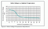
Therefore, if we use smaller Vcc, we get larger change in Ib, hence in Ic, hence in Vce, hence in bias point, just like MrAl has demonstrated it:
We can now immediately see that Vcc is in the denominator, so as Vcc gets larger the
magnitude of the change in Ib gets smaller. Thus a higher Vcc leads to less of a change
in Ib which leads to less of a change in Ic, which means less change in the bias point.

One thing that this circuit design is not a 'good' one is that the collector current depends heavily on the value of beta. Improvements can be made like audioguru suggested:
A properly biased transistor has a voltage divider feeding base current and an emitter resistor providing DC negative feedback.
 

Attachments

  • upload_2014-6-5_20-59-5.png
    upload_2014-6-5_20-59-5.png
    18.5 KB · Views: 278
Hi,

Looks good Heidi :)

I might add a little, that when we do this kind of thing it's just like taking a derivative of a function like:
y=2*a*b*c^3

We can take the derivative of y with respect to a, b, or c, and get different or the same results. But when we take the derivative with respect to any single variable we hold the other variables constant. So it's just a matter of keeping some constant.

dy/da=2*b*c^3 we keep b and c constant..
dy/db=2*a*c^3 we keep a and c constant.
dy/dc=2*3*a*b*c^2 we keep a and b constant.

If we had more variables, y=a*b*c*d*e*f
and we wanted dy/da, we'd keep all the others constant.

In our case, we wanted dIb/dVbe, so we keep all variables except Vbe constant.
 
Thank you, MrAl.

So the procedures we took might be an example of a physical interpretation of partial differentials, I guess.

One interesting thing I also notice, which you told me but I didn't get the point at that time, is that the collector/base current is always the same in every single experiment, this is because that's how we choose pairs (Vcc1, Rb1, Rc1), (Vcc2, Rb2, Rc2)...when we set Ic/Ib a fixed value. This can also be seen from equations (1), (2)
Rc= (Vcc-Vce0)/Ic0
and
Rb=(Vcc-Vbe0)/Ib0

... But to analyze over two or more different Vcc, we set up any experiment such that it always has the exact same initial base current. The base current is only allowed to change when we change Vbe, not when we change Vcc, because we dont change Vcc yet.
 
Hi,

Yes that is interesting, and the initial base current is made the same in each experimental circuit because that's how we would design each circuit with the different Vcc's, and this leads to the simplification of the diode in series with a resistor without even considering a transistor anymore. It boils down to a resistor in series with a diode where the initial current is the initial base current (now the initial diode current) and Vbe is just the diode voltage Vd, and now we let the diode voltage Vd vary instead of the base emitter voltage. If you do the math you get the same result. So really we are most concerned with what we allow the input to do and how it responds to a change in base emitter (or just diode) voltage.
The following is how I understand your resistor-diode simplified version (actually you have mentioned this simplified analysis in post #13, but again, I didn't get the point at that time. I appreciate your patience in guiding me throughout the analysis process):

In post #31, I listed two equations,
Rc=(Vcc-Vce)/Ic (1)
Rb=(Vcc-Vbe)/Ib (2)
But after that, I only focused on equation (2), because, like you said, we only need to consider the base current in this case.

So I think equation (2) is the math representation of the series battery-resistor-diode circuit.

Doing math on equation (2):
So for each Vcc we calculate the change in diode current,
In experiment #1:
Ib1=(Vcc1-Vbe1)/Rb1 or Ib=(Vcc1-Vbe)/Rb1 or Ib=(Vcc1-Vbe)/((Vcc1-Vbe1)/Ib1)
|dIb/dVbe|=Ib1/(Vcc1-Vbe1) --- (3)

In experiment #2:
Ib1=(Vcc2-Vbe1)/Rb2 or Ib=(Vcc2-Vbe)/Rb2 or Ib=(Vcc2-Vbe)/((Vcc2-Vbe1)/Ib1)
|dIb/dVbe|=Ib1/(Vcc2-Vbe1) --- (4)
then compare those two currents to find out which one changed the most.
Compare (3) with (4), variation in Ib is larger when Vcc is smaller, that is undesirable.
The one that changed the most is the worst because that means the bias point changed the most and we dont want that.
 
Last edited:
Hello again Heidi,


That looks good too. Your English seems very good too so it is hard to tell you had a different first language.

I found another 'example' that is a little different, but does involved some context or viewpoint that we have to realize before we can make any real sense of it. Im not sure if you are interested in seeing this or not so i'll wait to post any pic.

What it was, was a graph of strike voltage vs ambient temperature. I was looking at some fluorescent tube data recently because i was fixing a tv set with a fluorescent backlight and i found that graph.
At first it seems like it is a graph of the strike voltage as compared to the normal power supply voltage, so it would be the variation of strike voltage as the temperature changes but with a certain but unspecified power supply voltage. But what it really is is a graph of strike voltage as the temperature changes but relative to the strike voltage itself. So what they vary is the temperature but show how much the strike voltage changes relative to what it is at some normal temperature like 25 degrees C.
Again i had to identify what was constant and what was changing, and understand the 'context' of what they were trying to get across with this graph. I could have easily made the mistake of thinking that it was relative to the normal power supply voltage.
 
Thank you, MrAl. Chinese is my native language. My English is not good at all, I'm still learning, I can only read and write simple and straightforward sentences.

As you can see, I'm just a beginner in Electronics, I don't know what a strike voltage is, but I can imagine a 3-D coordinates system which might be used to depict what you described, if I understand them correctly:
so it would be the variation of strike voltage as the temperature changes but with a certain but unspecified power supply voltage
upload_2014-6-7_20-43-15.png


But it seems to me from your description that you found the strike voltage was actually rising, say, 0.01V for every degree of temperature rise from 25°C, for example.

I'm curious to see what graph it was, how you recognized what was constant and what was changing and how you decided what was the appropriate context.
 
Last edited:
Hi,

Here's the graph. I know it's not exactly the same thing we had been looking at, but it is similar in a way in that you have to figure out what they are trying to accomplish or say about a circuit.
Note the word "Normalized".
 

Attachments

  • StrikeVoltage-1.gif
    StrikeVoltage-1.gif
    35.5 KB · Views: 294
At first glance, it is dimensionless on the Y-axis and there's a '%' symbol there, so I guess the Y-axis must indicate a ratio, maybe a ratio of strike voltage to something.
The question is a ratio of strike voltage to what?

Yes, I think the key is the word normalized, this terminology normalized voltage must have a special definition.

Then, I think I found the answer, "Normalised" means "relative to some specified reference value," and more at https://electronics.stackexchange.c...c-current-gain-as-oppossed-to-dc-current-gain

Back to the StrikeVoltage graph, at 28°C, it has a value of 100% or 1, so I guess the strike voltage has a particular value, V28 for instance, specified somewhere else.

Around 36°C ~ 40°C, the value on Y-axis is about 99% or 0.99, therefore the strike voltage is (V28*0.99) around 36~40°C.

I guess the graph is a (strike voltage/strike voltage at 28°C) vs temperature one.

If what I conjectured were right, the constant would be the strike voltage at 28°C, and the variables would be temperatures and the corresponding strike voltages.

"They could have just used the actual strike voltages at various temperatures," why are they always making things complicated? I can't help wondering : (
 
Hi again,

We crave constant things in life, so when something is not constant it bothers us a little sometimes because it takes a little longer to interpret. We would rather go to the store and see a price of 50 cents per apple when we want to buy one apple than to see a price of 5 for $2.49 because we know right away what the price of one apple is without having to think about anything.

As for the 'graph', believe it or not, showing the data that way actually makes it easier to represent every tube ever made. The reason is because there are other variables, and in order to show the way it changes for every tube without having to list every single voltage, a single graph does it.
For example another variable is tube length, and the strike voltage goes up with tube length too, and there are lots of tube lengths to consider. A tube of 200mm might require a strike voltage of 650 volts at 25 degrees C, while a tube of 400mm might take a strike voltage of 1100 volts at 25 degrees C. For these two tubes alone we would have to create a table showing the voltages of both tubes as the temperature varies between two significant levels. Imagine if we wanted to show every tube in this table. But instead, one graph shows all the tubes so when you go to design something in your country you can look at the same graph for your 200mm tube as the guy in Japan when he goes to design his product using a 400mm tube.
Yes, we can make a table, and show every tube with say length increments of 10mm or something like that, but we dont really need that if we just learn how to use the graph.
This is how many specifications are shown anyway for electronic products.
 
Status
Not open for further replies.

New Articles From Microcontroller Tips

Back
Top