Roff
Well-Known Member
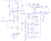
OK, here it is.
This works by generating a linear ramp on C1 with the current source made up of U1a, Q1, and associated components. The final amplitude of the ramp will be proportional to the pulse width. The peak amplitude will be held on C1, buffered by U1B, and sampled and held by U2d and C2. The held voltage is amplified by two in U1c, with an offset generated by D3 and U1d to subtract out the minimum voltage of about 2.5V, corresponding to the minimum pulse width of 1ms. After sampling, C1 is discharged by U2c to get ready for the next pulse. The timing for the sample pulse and the discharge pulse is created by generating another ramp (with current source Q2 and cap C3) that is as long as the time between pulses (2ms nominal - if this changes much, the timing generator will have to be modified). The two window comparators U3a/U3b and U3c/U3d create the discharge and sample pulses, respectively.
The 1% resistors and the COG (NPO) capacitor are for stability. If this is not important, you can use sloppier parts.
Calibration can be done several different ways. The simplest may be to lift one end of R12 (you could add a series pushbutton switch), set the input pulse width to 1ms, and adjust Re2 for 2.50V on the output. Then reconnect R12, set the input pulse width to 2ms, and adjust R13 until the output is at 5.00V.
The quad op amp can be changed, but the critical parameters are 9 volt supply capability, very low bias current, input common mode range within 1.2V of VCC, and output range zero to VCC-1V. A rail-to-rail I/O part is the simplest to find, but I don't know if you can find one that is not SMT. You can obviously use op amps in separate packages.
Don't forget to add power supply decoupling capacitors.
") kind of a roundabout way of doing it, but it's sure simple, and you can get cheap servos for like 8 bucks, and the motor and gearbox without electronics are great for robotics/etc too
kind of a roundabout way of doing it, but it's sure simple, and you can get cheap servos for like 8 bucks, and the motor and gearbox without electronics are great for robotics/etc too ")
