Continue to Site

Welcome to our site!

Electro Tech is an online community (with over 170,000 members) who enjoy talking about and building electronic circuits, projects and gadgets. To participate you need to register. Registration is free. Click here to register now.

  • Welcome to our site! Electro Tech is an online community (with over 170,000 members) who enjoy talking about and building electronic circuits, projects and gadgets. To participate you need to register. Registration is free. Click here to register now.

Pulse transformer / coil tester - slow turn on

Status
Not open for further replies.

MacIntoshCZ

Active Member
Hello,
i am missing something =).
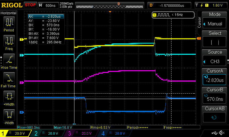
On channel 2 is overshoot
some capacitence is charging
ch4 is green
thanks for help
DS1Z_QuickPrint25.png
1-page-001(1).jpg
1605440773118.jpg
 
Very good pictures.
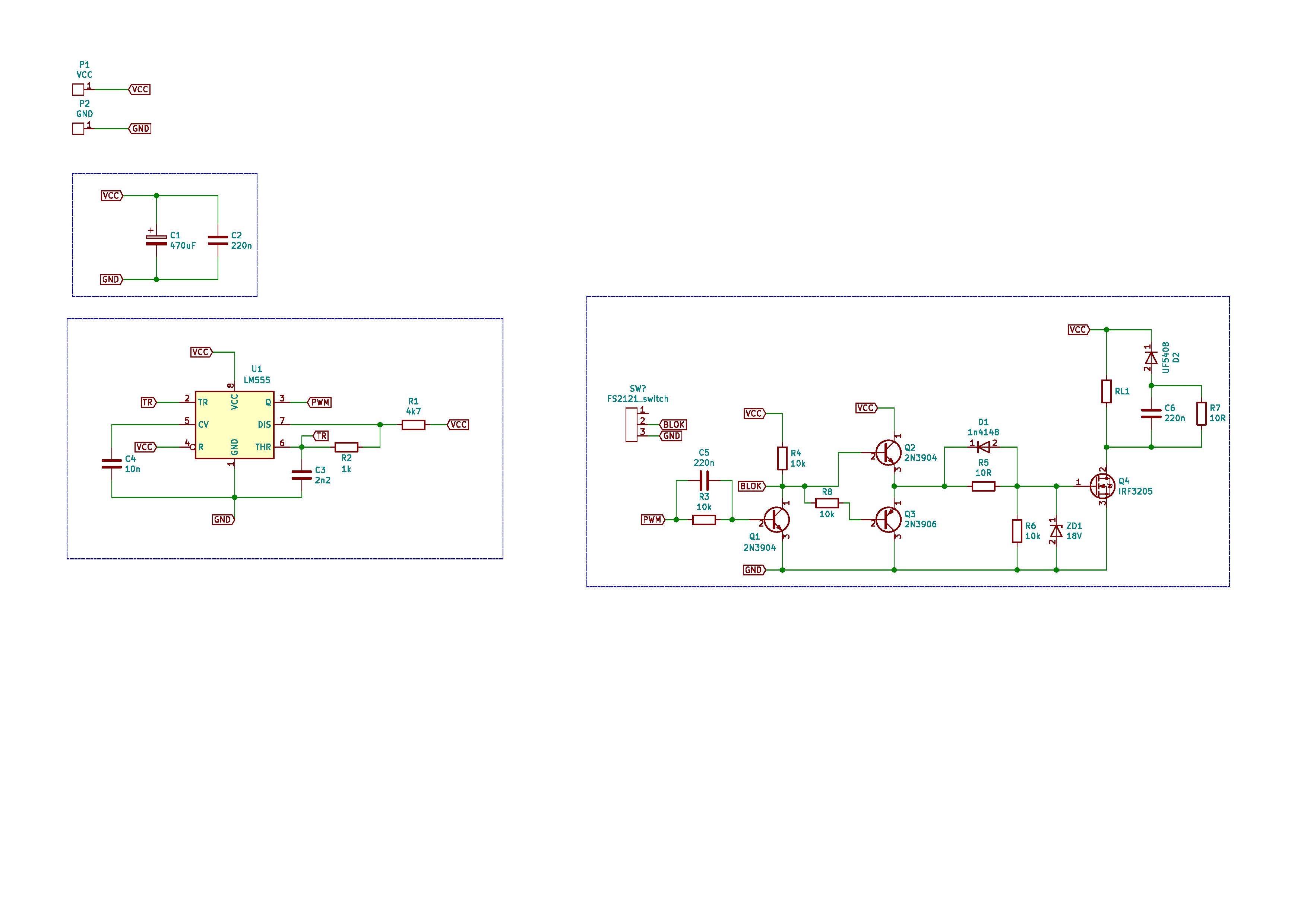
R8 should be 0 ohms. It slows down the fall time of the Gate signal.
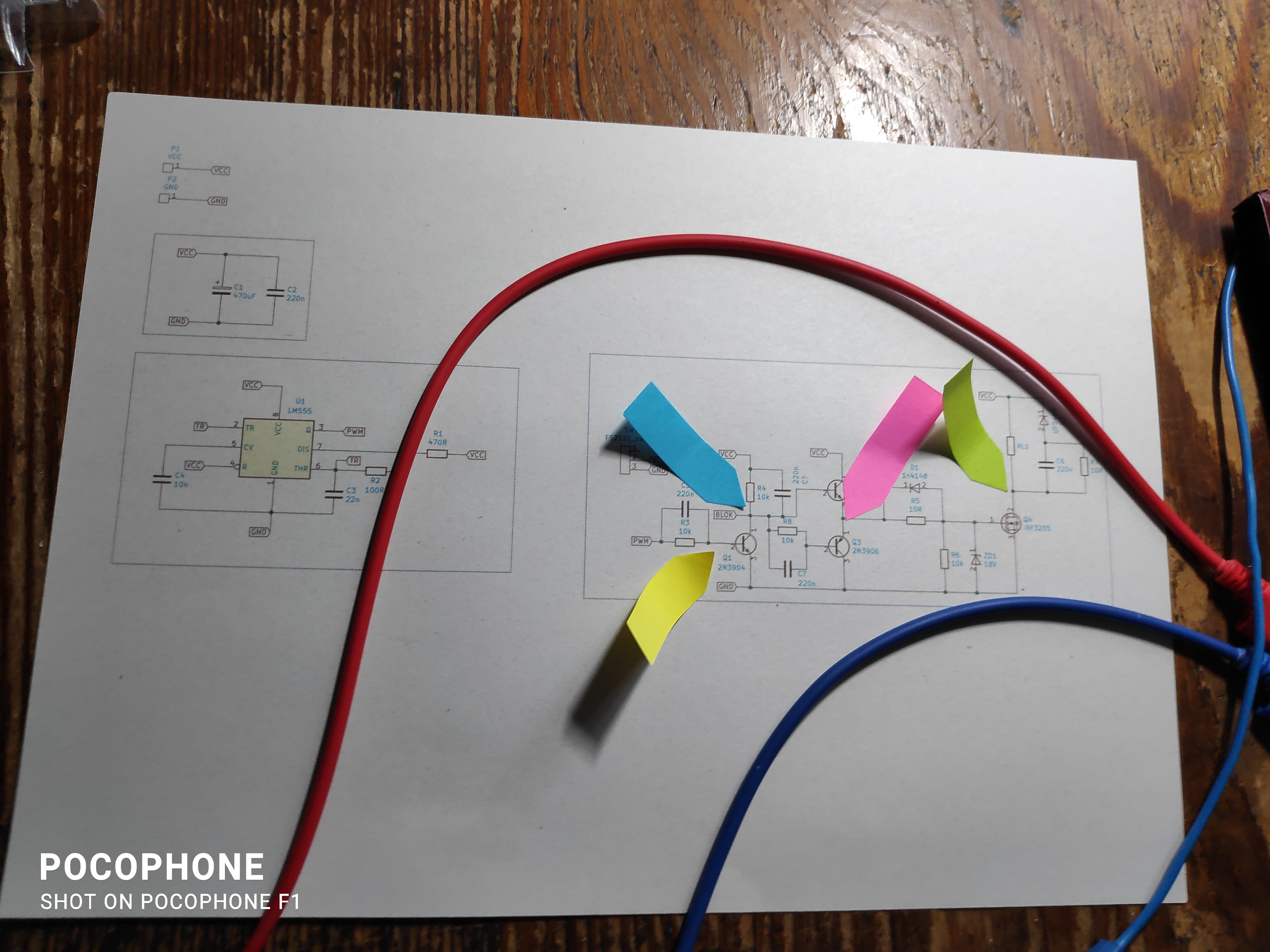
R4, in the paper schematic, has a capacitor across it. Bad idea.
R8, try 1k to increase current.
 
Very good pictures.
R8 should be 0 ohms. It slows down the fall time of the Gate signal.
R4, in the paper schematic, has a capacitor across it. Bad idea.
R8, try 1k to increase current.
Sorry i forgot to mention that circuit printed on paper was faulty. Actuall Schematic of PCB Is printed to jpg And attached. So parts without numbers are not added to PCB.
 
Is the "pwm" signal travelling along one of those long wires in the paper schematic photo? That could be part of the problem. (I'm going on the basis of ringing in the blue trace, although that trace is lagging - are you sure you labelled them correctly?)
 
I think you need to re-work the source pin joint on the mosfet - it looks like the pin didn't heat up enough when you soldered it (I'm not too clued up on mosfets and might have called it the wrong thing - I mean the one soldered to the ground plane anyway)
 
I think you need to re-work the source pin joint on the mosfet - it looks like the pin didn't heat up enough when you soldered it (I'm not too clued up on mosfets and might have called it the wrong thing - I mean the one soldered to the ground plane anyway)
I can see that joint doesnt look best :D. But it Is joint from 220n cap. I Will repare IT anyway.
 
Huh? I definitely mean the pin connected to the ground plane, not the cap. The pin on the right as you look at the writing on the transistor.
 
I think that maybe "Q1" 2n3904 is too slow for low current base driving. 200ns+ delay?
 
I wondered about it but assumed it's a published design so they would be correct. But actually if your switching 20v it may well be inadequate. Bear with me a minute whilst I fire up LTSpice...
...ok this is taking longer than expected...
and leads to more questions...
So, the yellow trace is the base of Q1, yes? I don't see how you are getting a negative-going pulse there, since the output of the 555 should be positive-going.
The collector of Q1 is also negative going, which is correct. So either there's something wrong there, or you have channel 1 on the 'scope inverted, or you've build a part of the circuit which isn't present, or probed the wrong spot.
I used 1mH with 60R in series for the relay coil.
Ok, the simulation shows a reasonably clean signal so far. Also, the output of the totem-pole in the simulation is ok and synchronised with the input. It's showing total lag between input and output of a few hundred nS. Certainly nothing like the signals you are seeing.

Anyway, it confirms those transistors are up to the job and validates the design - well, as much as it can anyway.

I would re-check all the connections very carefully, look for solder bridges, or other shorts, open traces, check all the components are actually the values they say they are, and confirm that the transistors do actually work and that you have actually wired the circuit the way you think you have. As a low budget experimenter, I speak from experience....
It was inverted. Jesus... Huge sorry And Also huge thanks for your time. It surprise me that it works in simulation. At the moment everything i designed needs an improvment after realization :). Its not Schematic from internet i just sit to computer And draw something using scrap parts from old psu (no 555). So i am little bit sceptical about used parts. Do you remember switching frequency (something around 100khz)? My pcb has 65khz. Thats weird
 
I had made measurement Once again And i dont think that it was inverted as you can see on M1 CH 2.
 
Ok I'm getting confused now (it doesn't take much!). So in measurement 1, what is the yellow trace actually showing? You've marked the pwm output with yellow, but the trace is the wrong way up! However in M2 the output looks ok but I don't see how the blue trace is managing to be a time traveller.
Also in M2, the output - pink/purple trace should be the same polarity as the pwm signal since it's inverted twice, yet it's the same polarity as the blue trace which you are showing as the gate of the mosfet.

I really suggest that if you haven't already, you download LTSpice from Linear Technology and simulate this circuit. Don't worry about getting models of the exact same components, similar will do. It's a big help predicting what your signals should look like.
 
Several things need changing.
1) C5 from 220nF to 100pf. You have a very large cap there and are driving the base below ground by 9 volts. The base should never see more than -5V. It damages the base and kills the gain of Q1.
2) As I stated before there is no enough current in Q1-C to make the part run fast. R4 from 10k to 1k. (rise time problem)
3) As I stated before R8 should be removed. With 10k Q3 is not turning off in time. (rise time problem)
1605674537363.png
 
Several things need changing.
1) C5 from 220nF to 100pf. You have a very large cap there and are driving the base below ground by 9 volts. The base should never see more than -5V. It damages the base and kills the gain of Q1.
2) As I stated before there is no enough current in Q1-C to make the part run fast. R4 from 10k to 1k. (rise time problem)
3) As I stated before R8 should be removed. With 10k Q3 is not turning off in time. (rise time problem)
View attachment 128092
Thanks i will replace all components as you mentioned. I tried before just put another 10k across R4 and it did some strange things. It makes turn on larger and when i touch it with finger than it completely dissapear. Body capacitence to ground?
 
Status
Not open for further replies.

Latest threads

Back
Top