Continue to Site

Welcome to our site!

Electro Tech is an online community (with over 170,000 members) who enjoy talking about and building electronic circuits, projects and gadgets. To participate you need to register. Registration is free. Click here to register now.

  • Welcome to our site! Electro Tech is an online community (with over 170,000 members) who enjoy talking about and building electronic circuits, projects and gadgets. To participate you need to register. Registration is free. Click here to register now.

prototype pcb design

Status
Not open for further replies.

earckens

Member
How would you approach the design of such a protoype pcb with Eagle?
1. straight to "new - project", "new - schematic", "new - board",..?
2. create repetitive pads and vias, no vias (the board my be single sided)?
3. copy from someone, somewhere?

Thks, Erik
 

Attachments

  • ecs3-h.jpg
    ecs3-h.jpg
    79.2 KB · Views: 266
My first prototype was on strip board.... Then made a single sided etched board... When I was happy I had 100 made..
I have always used Protues... Even back at Uni, so it was reletively easy.. However!!! Even when you have your first production run, you will find something Doh!!!

I'm on my 3 series.... Does get easier!!
 
Aberlour, .. you know Ardbeg Uigeadail? I have one here; amongst others.

How does your prototype pcb look like? Protues, what is that?
 
How would you approach the design of such a protoype pcb with Eagle?
1. straight to "new - project", "new - schematic", "new - board",..?
2. create repetitive pads and vias, no vias (the board my be single sided)?
3. copy from someone, somewhere?

Thks, Erik

This is only my view:

In any ECAD system the schematic is always the reference. If you do not get that right you will have all sorts of problems. So it is essential to get the schematic perfect before attempting any PCB layout etc.

spec
 
Thank you, that is the input I needed. I did not know how to approach this.

But now, how do you start with a layout where there are no components, just a pcb with a bunch of pads and a repetitive numebr of little tracks in a fixed pattern?
 
Even when you have your first production run, you will find something Doh!!!

Isn't that the truth. I have found problems with designs that have been in production for a few years. The gremlins tend to creep out when you change PCB manufacturing houses.:arghh:

spec
 
Thank you, that is the input I needed. I did not know how to approach this.
Eagle should do this for you.... As Spec said do a scematic in eagle, then transfer to PCB layout and all the rats nests should be ready to route//
 
The gremlins tend to creep out when you change PCB manufacturing houses.:arghh:
Last batch had too much tin and I couldn't get the compnents in.... Moved to china, they seem to get it right!!
 
Thank you, that is the input I needed. I did not know how to approach this.

But now, how do you start with a layout where there are no components, just a pcb with a bunch of pads and a repetitive numebr of little tracks in a fixed pattern?
Hmm good question earckens. Afraid I don't know.

I will have to put my hand up and say that I have never done a PCB layout in CAD- someone else always did that at work. (I have done plenty of hand layouts though in the good ole days).

spec
 
Last batch had too much tin and I couldn't get the compnents in.... Moved to china, they seem to get it right!!
There is always something to catch you out. The favorite was to do a mirror image of the PCB.:D

When fine multilayer PCB manufacturing, with buried via holes, first became available, we used it for a particularly critical project: I think the boards were seven layers and the only company with the technology was in Sweden. I won't go into the details but we had problem after problem and the project slipped and slipped. We had meeting after meeting with many trips to Sweden. Finally after about nine months it was all sorted and we had our first board working on the bench- we all went down the pub for a celebratory lunch. Then the factory in Sweden burnt to the ground!

If the gods can't get you one way they will get you with another.:wideyed:

spec
 
When starting with a PCB layout you have to fist define the board size... There has to be a closed line that represents this.

Then when the schematic is ported across ( you can do PCB's from scratch, but it isn't recomended ) you can then optimise the component layout... Set the design rules, track widths etc...

Then hit autoroute... As autoroute is quite rubbish, you can start swapping routes to better serve you PCB....

Keep analouge and digital seperate and place many decoupling caps....
Make sure your ground rail is as big as you can get it... I try to make my power rails T30 or bigger..

I may do a video, Check out Jason's site.... I'm sure he has done vid's on this https://atomsoft.wordpress.com/?s=pcb+video If this isn't the one, there is certainly something here..
 
Never tried that whisky ... I'll have to give it a go..

I only prototpye on stripboard.. Once I'm happy it goes for manufacture... I never do etching anymore
If you like peat, great taste.

Manufacture: you mean you send the gerbers to a fab?
 
But I still do not know how to start with a schematic, without components, to be transferred to a pcb where I want repetitive patterns of holes, pads and interconnections between pads (see my picture in post #1);
 
By the way when you install EAGLE a user manual and tutorial also gets loaded. You can access this documentation from the EAGLE Control Panel (first panel that displays when you boot EAGLE).

spec
 
'IN PRINCIPLE, you can just create a board WITHOUT schematic (menu> File >

New >Board) and add your elements there, no problem.'


**broken link removed**
 
But I still do not know how to start with a schematic, without components, to be transferred to a pcb where I want repetitive patterns of holes, pads and interconnections between pads (see my picture in post #1);
So you want to make a stripboard??? May I ask why, when there are ones you can buy!!
 
First layout the board
upload_2016-10-14_13-26-32.png

Then add a T block (I chose an 18 way)
upload_2016-10-14_13-28-47.png

Then a simple replication
upload_2016-10-14_13-29-39.png

Lastly I place the traces.... T30 the T60 and T80 So you see the difference
upload_2016-10-14_13-30-52.png

Then print and make...
 
This would actually be simple in Eagle and can be done in a number of ways.

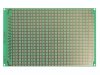
If I were doing this, I would first create a "package" in a new library. This would consist of 3 pads at 0.1" spacing of the appropriate diameter, with a trace connecting them. Draw a silk screen board around the group of three pads if you like. Save this package.

Next, create a new board and add the newly created library. Set the grid spacing to 0.1".

Select your newly created package and lay out a line of them, say 10 in a row to get 30 holes. With the grid spacing set to 0.1", this will be simple.

When the first row is to your liking, group the entire row, right-click over the first pad in the row, and click the cut symbol. Cut the group.

Click "paste" (I think it looks like a magic wand) and you'll have another row of pads. Position it 0.1" from the first (again, simple because your grid spacing is 0.1"). Repeat as many times as you line.

If you want to make continous "bus" strips at the top and bottom, duplicate the rows 2 more times. Then use the air wire tool to connect all the 3 pad groups in the row together and route a trace between them all.

If you need more details, I'd be happy to provide step-by-step instructions.

There may be one problem with your plan however. Do the low-cost board options have a limitation on either holes per square inch (100 in this case) or total number of holes in the board?
 
Status
Not open for further replies.

Latest threads

New Articles From Microcontroller Tips

Back
Top