great explanation, but i still have 2|3 doubts about the circuit...
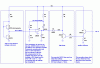
1.- the clip voltage (output) is as you point out Vref*(Rf/2.7k)+1 or Vref*((Rf/2.7)+1)
2.- I have problems understanding the function of D2 and D3, the anode of D3 is connected to a fixed voltage (i think) and it only conduces in one direction, from output to the output of the opamp(comparator). About D2 I simply don't know what it is doing there
")
3.- I suppose that R3 is the pull-up resistor needed by the open collector output of the comparator, am i right?
I think that's all, the main problem is with D2 and D3 and how changes the output.
thanks