Continue to Site

Welcome to our site!

Electro Tech is an online community (with over 170,000 members) who enjoy talking about and building electronic circuits, projects and gadgets. To participate you need to register. Registration is free. Click here to register now.

  • Welcome to our site! Electro Tech is an online community (with over 170,000 members) who enjoy talking about and building electronic circuits, projects and gadgets. To participate you need to register. Registration is free. Click here to register now.

PP3 - 555 LED flasher - negative voltage?

Status
Not open for further replies.

Fordy

New Member
Hey, I'm trying to sort out a PCB for a mate, running into a weird issue.

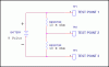
In brief, his circuit sources 9v from a PP3, going to three inputs (each OR latched) and then on to a 555 to flash a bank of LEDs.


The problem, is that while the PP3 is providing a pd of 9v, the +terminal is at 5.83v and the -terminal is at 3.16v.


The LEDs are solid on, no flash, whether input is on or not. Breaking the OR latch has no affect.

I believe this is because the gnd of each 555 is at -3.16v, so even if the input is off there is still a pd of 3.16v.


I have no experience with using -ve voltage though, and don't really understand it, so any help in fixing this would be appreciated. I know that you can get -ve by grounding the +ve terminal instead of -ve, but here the issue is that a single PP3 is providng both a + and a - which I do not understand.


Many thanks in advance.
 
Last edited:
Take a look at the attached drawing. If I take my common meter lead a place it on TP-2 and use my + meter lead and measure from TP-1 and TP-3 respectively what voltages should I read? The battery is a 9 volt battery.

There is no actual negative voltage in the circuit you have. It is a matter of the point of reference. When you took your readings where was your meter negative lead connected? Think about moving the meter leads around on the circuit I attached. How about if you place the negative lead on TP-1 and the positive lead on TP-3 what will a DMM read as to voltage?

A schematic of what you have would make it easier to get help and troubleshoot. Nobody here can see the circuit and your description doesn't quite get it.

Ron

Ron
 

Attachments

  • Voltage Divider.gif
    Voltage Divider.gif
    6.1 KB · Views: 307
I didn't place a DMM anywhere - this is in a simulator of the "Circuit Wizard" software package.


Pretty sure it is a negative voltage not point of reference - it's present throughout a huge chunk of the circuit.

I can't post a schematic because the schematic works fine - I did something wrong when making the PCB.

I can't demonstrate it properly in a pic, because it's just a messy PCB with no labels and a load of offboard components - but here's a screen shot with everything spread out a bit more.


I appreciate that it's impossible for you to follow, I just want to illustrate that it's not just a couple of points that are negative - in the shot below, everything blue is -3.16v.

And everything that's at -3.16v should be 0v. I just don't understand why it isn't.
 

Attachments

  • Untitled.png
    Untitled.png
    100.1 KB · Views: 241
Last edited:
OK, but as I said, the schematic when simulated works fine.

I've stuffed something up making the PCB. But I've dedone it twice and made the same mistake - whatever that is.


For what it's worth, I know this'd be much easier with a PIC. I've triedto convince him, but he wants it done with 555s.
 

Attachments

  • Untitled.png
    Untitled.png
    31.9 KB · Views: 247
Last edited:
OK, but as I said, the schematic when simulated works fine.

I've stuffed something up making the PCB. But I've dedone it twice and made the same mistake - whatever that is.


For what it's worth, I know this'd be much easier with a PIC. I've triedto convince him, but he wants it done with 555s.
There is no ground in your schematic. i have never seen a simulator that will run on a circuit which has no ground.
The negative terminal of the battery on the left hand side of the circuit would normally be designated as ground.
Also, your CD4071s have floating inputs, which is a no-no. The circuit's operation will be unpredictable unless you add resistors to one of the rails (probably ground, but I haven't analyzed the circuit to be able to say that definitively).
Your D2 LEDs have no current limiting, unless they have a built-in resistor.
The LEDs which are driven by the 555s should each have their own current limiting resistor. Parallel LEDs may wind up with one of them hogging most of the current, which will give them unequal brightness, and, depending on current rating, could damage them.
 
Last edited:
Uh, it's a PCB where would you suggest I put "a ground"?


Fair enough, the schematic doesn't, but it works as fine as I've already said. This simulator is obviously contrary to those that you've used.

The LEDs do have resistors. Parallel.. well that's a design choice - as I say it's a mates circuit not mine, I'm just doing the PCB.


I've rebuilt it again, works a bit better this time. The only issue is the emitter from transistors to 555 (and whole of the circuit after that) is bouncing around when the base is high. I'm sure that's a simpler fix but I'm too tired at the moment.
 
Instead of using a transistor to disconnect the power supply to each 555, use pin 4 of the 555.
 
I fixed the "bouncing around" - I'd left out the caps! Really was tired this morning...


Strange issue arose after that though - the LEDs were on solid when the should have been off. Still flashed as should, pressing the breaker sent them back to solid on.


Unwilling to fix it, I just stuck in a 4069 (hex inverter) at the end. Works fine now.

Negative voltage was sorted by removing the 6v supply that switched on the PP3 - I don't know why he had it in anyway, but once I removed it and made some other changes, it worked fine - I presume that's what it was down to.


Thanks for the help.
 
Have you fixed the floating inputs on your OR gates?
From my previous post:
Also, your CD4071s have floating inputs, which is a no-no. The circuit's operation will be unpredictable unless you add resistors to one of the rails (probably ground, but I haven't analyzed the circuit to be able to say that definitively).
 
Haha, no by "sorted" - I mean "sorted", thanks.


As in "it's fine". Cheers.
It won't be fine unless you have resistor (100k) to ground from each input. Sorting does not allow you to find the parts that don't need resistors. ALL CMOS gate inputs need to be connected to something that eventually has a current path to ground.
 
As I said before, that was already done when you picked up on it - by "sorted" I mean "everything is fine and it works".

The resistors weren't shown in the image you saw because that was the schem done by the mate that I'm doing the PCB for. I scratch built the PCB and made changes myself - such as the resistors to pull down to ground.


Thank for resonponding.
OK, now I get it. Here in the US, we don't use "sorted" in quite that way, although we do use it in the sense of "getting things sorted out", which could refer to getting almost situation in order, or figured out.
For future reference though, when you post a schematic, it would really help if it is accurate.
 
Last edited:
For future reference though, when you post a schematic, it would really help if it is accurate.


Look at what I originally said:

I can't post a schematic because the schematic works fine - I did something wrong when making the PCB.


I was never having an issue with a schematic - so that's why it "isn't accurate".

I never made a schematic for this project myself - the schematic I gave you in the end was the one I was working from to create a PCB for the buddy that made the schematic.


It was the same project, but I made some changes, such as adding in said resistors. I couldn't show that to you in a schematic because I never made one.
 
OK, I apologize for dragging this thread off topic. Did you ever get the negative voltage issue with the simulator figured out? If not - you must have had to use two probes, since there is no ground in the schematic. Where did you place the "common" probe (negative one, I would think)?
 
Yeah that works fine now too.

The way the software works there is no necessity to place one probe, let alone two. It simply shows the current and voltage throughout the whole circuit simultaneously, with numbers if you hover over, or a representation through a colour scale.


Varying shades of blue, green and red show varying intensity (voltage) of negative, ground and positive respectively. With current shown by the speed at which its flowing.


Quite a handy tool actually, you can quickly and easily see roughly what the levels are anywhere in the circuit at any time, when outputs are high or low etc.


It fixed after I re-did the circuit without the 6v battery - relay switching on the PP3. I guess there must have been an overlap somewhere there, causing a leakage of negative over the common track.
 
Status
Not open for further replies.

Latest threads

New Articles From Microcontroller Tips

Back
Top