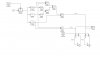
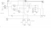
Continue to Site

Welcome to our site!

Electro Tech is an online community (with over 170,000 members) who enjoy talking about and building electronic circuits, projects and gadgets. To participate you need to register. Registration is free. Click here to register now.

  • Welcome to our site! Electro Tech is an online community (with over 170,000 members) who enjoy talking about and building electronic circuits, projects and gadgets. To participate you need to register. Registration is free. Click here to register now.

pipeline adc

Status
Not open for further replies.

texas007

New Member
Dear All,
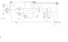
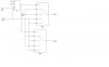
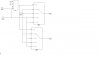
I am trying to implement a 10 bit ADC model in Simulink.
When the input voltage of 5V(sine wave) is provided the outputs obtained on the scope are all 1's(1111111111).When the input is changed to some other value such as 3V the output bits are something different than expected.
As per calculations:
Step size=5V/1023=0.00489.
if for 5 binary has to be 1111111111(1023)
For 3 binary 1001100101(613)
The binary output for 3 I am getting it as 1100110011 which equals to decimal equivalent of 819.
Please correct me what is going wrong in the method
Really need your help.
Thanks in advance.
 
Sounds like 3V is the RMS value and the ADC is measuring the peak value (613/819 = .748 which is near the ratio of RMS to peak of a sinewave).
 
Sounds like 3V is the RMS value and the ADC is measuring the peak value (613/819 = .748 which is near the ratio of RMS to peak of a sinewave).

Dear Carl,
Thanks for your input.But could you please elaborate on the above.I provided a constant dc of 3 also but I am still getting the same value as provided earlier by the sine wave.
Thanks once again.
 
If a 3V DC value gives the same output, that I don't know what's causing the reading you are seeing.

Can you post a schematic of what you are simulating?
 
If a 3V DC value gives the same output, that I don't know what's causing the reading you are seeing.

Can you post a schematic of what you are simulating?

Attached is the schematic for the stage 1 of pipeline ADC.
 

Attachments

  • stage1_pipeline.jpg
    stage1_pipeline.jpg
    49.8 KB · Views: 197
Attached is the schematic for the stage 1 of pipeline ADC.

Sorry to provide incomplete information.The input maximum voltage is 0.5 constant.The value for 0.5 after error correction is all 1's.The value obtained for 0.4 or 0.3 is not as required after error correction.Attached is also the error correction block used for this ADC.
 

Attachments

  • correction_error.jpg
    correction_error.jpg
    34 KB · Views: 168
I am unable to understand the operation from the schematics. Do you have a block diagram of its operation that you can post?
 
I am unable to understand the operation from the schematics. Do you have a block diagram of its operation that you can post?

Dear Carl I tried attaching the file.But I think it does not allow me to upload zip or rar compressed files.
Is there a way I can send you the file for your reference.thanks in advance.
 
Attached are 3 blocks of the model.The input is given to the PIP_STAGE1 either a sine wave or a dc voltage.This stage consists of a sample and hold,SUB ADC and Sub DAC.The bits from Sub ADC D1 and XOR output are send to the delay blocks.The delay blocks are provide delay to each stage from 9,9 to 1 delay cycles.The last stage of the input stage is a 2 bit flash ADC
The output of the delay blocks are given to the error correction.The 2 inputs to the error correction are from the delay blocks.the 10th bit is not passed through the error correction.The final outputs obtained from the error correction is sent to he scope.
Let me know if any more info is required of me.Thanks a lot once again.
 

Attachments

  • PIP_STAGE9.jpg
    PIP_STAGE9.jpg
    49 KB · Views: 176
  • PIP_ERROR.jpg
    PIP_ERROR.jpg
    34.3 KB · Views: 157
  • PIP_STAGE1.jpg
    PIP_STAGE1.jpg
    59.4 KB · Views: 169
I am unable to understand the operation from the schematics. Do you have a block diagram of its operation that you can post?

Dear Carl,
I would really be glad if you could please help me out in this pipeline ADC in fixing the possible error.Its like a block and I am not able to fix it.Thanks a ton in advance.
 
I am unable to understand the operation from the schematics. Do you have a block diagram of its operation that you can post?

Hello Carl,
Please find attached the schematic for the pipeline adc.This is for each stage.so that a 1.5 bit/stage is produced.
 

Attachments

  • 1.5bit.jpg
    1.5bit.jpg
    28.4 KB · Views: 208
I'm afraid that I don't have time to analyze this rather complex circuit in detail.

Try to follow the signal through the simulation and see if you can determine where it may be misbehaving. Look at each stage and see if it's doing what you think it should at that point.

Perhaps someone else has some suggestions.

Good luck.
 
Status
Not open for further replies.

Latest threads

Back
Top