Wirth's Law
Member
Hello all,
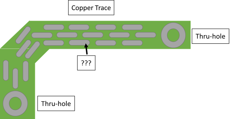
I was looking at a couple of used circuit boards, and on it I found several high voltage traces (120/240 VAC) with a strange pattern overlayed. Instead of being normal, solid green traces, they had a gray and dashed pattern on top, with the remaining copper covered with green solder mask like normal. It was as if the solder mask for this part was perforated in order to leave an exposed pattern of tin solder when the board was finished. I've attached a rough sketch of what it looked like.
Checking Google, I found some pages on circuit board features called thieving and stitching. But, I'm not convinced either of these are what I've seen on this trace, although they have similar purposes. I can guess at the moment that this might have something to do with thermal management, since the exposed solder should offer less thermal resistance to ambient temperatures, and because these traces carry the most current on this board.
So has anyone seen this before? Is there an industry-recognized name for this pattern/technique? And what purpose does it have?

