Continue to Site

Welcome to our site!

Electro Tech is an online community (with over 170,000 members) who enjoy talking about and building electronic circuits, projects and gadgets. To participate you need to register. Registration is free. Click here to register now.

  • Welcome to our site! Electro Tech is an online community (with over 170,000 members) who enjoy talking about and building electronic circuits, projects and gadgets. To participate you need to register. Registration is free. Click here to register now.

PCB Layout Puzzle

Status
Not open for further replies.

jack0987

Member
I only have one sided PCB board.
I wanted to connect the dots, so to speak, with as few jumpers as possible and found myself scratching my head.

Using the image on the left, I came up with a possible PCB layout on the right.
The 5 jumpers are in green.
I'd like the output order to be 1 to 8 and not 8 to 1 but can work with the 8 to 1.

Anyone like to take their hand at it?
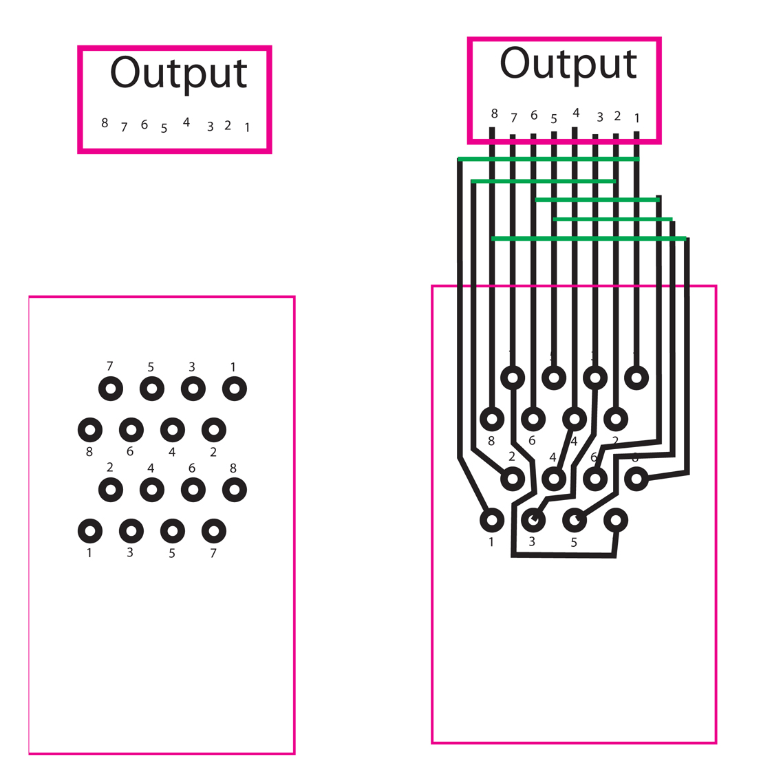
119567
 
I dont get what it is your doing. If your stuck with that layout and pcb already your going to be stuck with using jumpers and not much better can be done. Personally I would make a better board.
 
Last edited:
Im assuming the bottom part is a footprint you can not change and that the top part is some type of header for output and not just straight wires going out( and hopefully not edge pins)... If so you can fit it all on the board similar to this. Please excuse the sloppy routing. If you take your time you can clean it up, make it prettier and get it a lot tighter.

Forgot to label but is the same as your picture with output 8-1.
dddd.jpg


Here is one with the outputs switched to 1-8
cccc.jpg
 
Last edited:
I would turn the bottom connector 180° And relabel the pins.

1DA77843-F1E6-4D1D-B4E9-AA820B9B70F4.jpeg
 
Last edited:
Im assuming the bottom part is a footprint you can not change and that the top part is some type of header for output and not just straight wires going out( and hopefully not edge pins)... If so you can fit it all on the board similar to this. Please excuse the sloppy routing. If you take your time you can clean it up, make it prettier and get it a lot tighter.

Yes the magenta outlined pads are a footprint and can not be changed. The blue square is the PCB edge.

This is a better representation.
Pins 9 and 10 of the output connector are not used.
I did not think about going around the output pins at first. Thanks.

119581
 
Have you checked how much a double sided board will cost you? For example, here, I can get ten double sided boards 100mm X 100mm for $17.

Mike.
 
Have you checked how much a double sided board will cost you?
You don not want to put connectors on a single sided board. A single sided board, the connectors will only last a couple of times before the solder breaks. A double sided board is much stronger at the solder joints.
----edited----
If you are going to stay single sided, make the pads as large as possible.
 
Well I'd never made PCB's until recently, and I exclusively use JLC PCB for them, excellent quality and fast service - I've ordered some more today.

Last week I ordered some Monday afternoon, and the boards arrived Friday morning - can't grumble at that, we pay for DHL delivery, and the boards cost about "4 for ten, and about £16 delivery :D

However, I'm with everyone else - make it double sided, not worth messing about with single sided if you're having the boards professionally made.

However, if you really, really, want to make it single sided - design it as double sided, ensuring the top tracks are straight and don't block any components, then simply remove the top tracks and replace them with wire jumpers :D
 
I think the price at jlcpcb is the pretty much the same for 1 or 2 layers. No sense not using both sides since it looks to be through-hole anyway.
 
Last edited:
I think the price at jlcpcb is the pretty much the same for 1 or 2 layers. No sense not using both sides since it looks to be through-hole anyway.

As far as I know it is, but I was more thinking if he was making his own board at home.

I wouldn't consider ordering a single sided board from JLC, even though many of my boards are pretty close to SS anyway, and could easily be made so - but there's just no point, if you've got to solder a single wire link on the board it's an extra assembly step, for zero gain.
 
You don not want to put connectors on a single sided board. A single sided board, the connectors will only last a couple of times before the solder breaks. A double sided board is much stronger at the solder joints.
----edited----
If you are going to stay single sided, make the pads as large as possible.

You have a very good point. I will be making these PCBs here this time. Since they are for personal use they will not see heavy usage. I do make the pads bigger, use extra solder, and wrap a wire tightly around them through the circuit board and solder that too.
 
I only have one sided PCB board.
I wanted to connect the dots, so to speak, with as few jumpers as possible and found myself scratching my head.

Using the image on the left, I came up with a possible PCB layout on the right.
The 5 jumpers are in green.
I'd like the output order to be 1 to 8 and not 8 to 1 but can work with the 8 to 1.

Anyone like to take their hand at it?

View attachment 119567

Try rotating the bottom part 180 degrees..

eT
 
Status
Not open for further replies.

Latest threads

New Articles From Microcontroller Tips

Back
Top