I've created PCB's before with all through hole components and it was fairly easy to do. I used PCB Express software and services. I ran all of my power and ground traces on the bottom surface and all of my signal traces on the top surface. It was pretty straightforward.
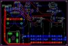
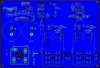
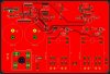
Now I'm trying to build a very small device and I'm laying out my PCB. I went to a combination of surface mount and some through hole components to save space. The problem I'm having now is that I can't get away from daisy chaining power and ground traces. With the combination of components I have to use and their necessary positions on the board, I'm having to use several vias and there is hardly a straight trace anywhere on the board.
I've read that I'm not suppose to daisy chain power and ground traces but I just can't seem to avoid it with this project. What are the dangers of doing so and what do I have to really watch out for at a minimum.
Thanks.