Continue to Site

Welcome to our site!

Electro Tech is an online community (with over 170,000 members) who enjoy talking about and building electronic circuits, projects and gadgets. To participate you need to register. Registration is free. Click here to register now.

  • Welcome to our site! Electro Tech is an online community (with over 170,000 members) who enjoy talking about and building electronic circuits, projects and gadgets. To participate you need to register. Registration is free. Click here to register now.

Op-amp to headphones: Forget Matching?

Status
Not open for further replies.
Yeah, I made a mistake in that drawing and had the base biased into V+ instead of a lower source. I checked out a few feedback topologies and found a simple fix that's supposed to lower crossover distortion and that clipping effect.

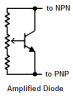
In general, are these 2 diodes a good way of removing crossover distortion? I found other versions that use biased transistors and even op-amps. But in general does this diode layout work?
 
2 diodes might match the two output transistors and work well.
But their forward voltage is a range and so is the forward voltage of the transistors.
So they might create a current that is too low which causes crossover distortion. Or they might create a current that is too high which causes a high idle current and a lot of heat.

The transistors get hot when they work hard then they conduct more which makes them hotter which makes them conduct more which makes ... themal runaway. An adjustable transistor "diode amplifier" bolted to the heatsink of the output transistors is much better than two diodes.

The 3 transistor power amplifier is crap. It has a very high amount of distortion.
 
What exact is the "diode amplifer?" If I use it along with a feedback loop, would that solve the distortion and runaway problems?
 
An amplified diode has other names. It is a transistor with a voltage divider at its base and either is set to a certain voltage between its collector and emitter or has a pot to set the voltage. The voltage sets the idle current in the output transistors. If the transistor has a heatsink tab then it can be bolted to the heatsink for the output transistors so its voltage follows the voltage of the output transistors as it changes with heat to keep the idle current constant and to prevent thermal runaway.

A low distortion power amplifier has many transistors so that some are linear current sources instead of resistors, and so that each one has local negative feedback. Your power amplifier has only 3 transistors so it has high distortion.
 

Attachments

  • amplified diode.PNG
    amplified diode.PNG
    3.2 KB · Views: 212
Okay. Yeah, that's what they called it in my Sedra & Smith reference, the Vbe multiplier. I'm probably going to use 2N3904/6 transistors for the final output stage. I have a supply of heatsinks that are made specifically for that To-92 package. If I were to solder these heatsinks together, would it provide the kind of thermal coupling I would need?
 
A TO-92 package is plastic-epoxy and doesn't conduct heat to a heatsink very well. But a little better than nothing.
 
That's a good point. I might have a few of those "metal can" types in the form of 2n2222's and 2n2907's but I don't know if those are closely matched. Otherwise, I could maybe take the two plastic cases and wedge a thin copper sheet in between them.

There's this other thermal shutdown feature I want to try out. It would add a 4th or possibly 5th transistor but it's making the math ugly.
 
Why are you making a horrible amplifier with transistors like they did 44 years ago? Now there are excellent inexpensive amplifier ICs.
 
I need to do more linear engineering. If I can do this at the discrete level, embedded chips would a walk in the park.

Secondly, I want to finish it using only parts I have on-hand. I can always re-visit this project and do a high-performance version when I have more resources available.


The thermal runaway issue raised another question for me. How do you simulate thermal runaway? Is there software for it, or is it experimental-only?
 
I don't know if temperature effects can be seen on simulation software.

I have made many amplifiers with transistors. The simple one with only 3 transistors sounds very distorted. I made some amplifiers almost the same but with two extra transistors so that the outputs are Sziklai pairs and the distortion is much lower. I simulated it (I should have added emitter resistors):
 

Attachments

  • Sziklai pairs.PNG
    Sziklai pairs.PNG
    24.3 KB · Views: 224
I should have added emitter resistors
Yes, emitter resistors are important here. Without an emitter resistor, Q1's operating point is all over the place depending on its beta. (I would also have a resistor from Q1 base to 0V.) And without emitter resistors, the output stage is very temperature sensitive.

@ag: Would be fun if you posted the .asc file so I could play with the ckt without re-entering it.
 
mneary said:
Yes, emitter resistors are important here. Without an emitter resistor, Q1's operating point is all over the place depending on its beta. (I would also have a resistor from Q1 base to 0V.) And without emitter resistors, the output stage is very temperature sensitive.

@ag: Would be fun if you posted the .asc file so I could play with the ckt without re-entering it.
Q1 has lots of negative feedback from the output instead of from an emitter resistor so its operating point doesn't change much with beta changes.

Here is my sim file:
 

Attachments

  • sim bootstrapping.asc
    3.1 KB · Views: 194
Thanks for the .asc file!!!

The circuit is designed for a Q1 beta of about 200. If the beta is maximum (300) then it operates at a center of 3.5V. If it's at minimum (50) then the center is about 6V. For a headphone amp this is probably OK.

[edit] Obvious to almost everyone, but I'll mention anyway: If this circuit is used with almost any power source (especially an alkaline battery, 9V should be bypassed with a capacitor, maybe 1000uF. [/edit]
 
Last edited:
If I restrict the input signal so that the my output is close to 1.1Vrms, would this reduce any distortion even further?
 
Maxim

bananasiong said:
**broken link removed** has got it solved.

We were using Maxims on our serial communications when I was in manufacturing they held up better all around.

What I mean (is) this product had some real problems with startup voltages that would normally take anything else.
 
DigiTan said:
If I restrict the input signal so that the my output is close to 1.1Vrms, would this reduce any distortion even further?
When you reduce the input signal then the output level and distortion are also reduced.
 
I noticed the 2N4403/2N4401 have higher absolute max collector currents. Is that why they were placed on the output instead of 2N3904 and 2N3906?

Also since the bootstrapping stage is a class C amp, will the input be allowed to dip below 0V?
 
Last edited:
The peak voltage across the 8 ohm load resistor is 3.3V so the peak current is 413mA which is too much for 2N3904 and 2N3906 transistors.

Class-C amplifiers are not used for audio. Too much distortion.

The bootstrapping dynamically increases the supply voltage for the resistor that feeds base current to the NPN output transistor so its distortion is much less.
The voltage gain is more than without boostrapping and if the gain is reduced then the distortion will be even less.
 

Attachments

  • bootstrapping.PNG
    bootstrapping.PNG
    45.1 KB · Views: 226
Did the value of that bootstrapping capacitor have to calculated or is there a rules-of-thumb? It seems like you'd have to take an RC time constant into consideration.
 
Status
Not open for further replies.

Latest threads

New Articles From Microcontroller Tips

Back
Top