Continue to Site

Welcome to our site!

Electro Tech is an online community (with over 170,000 members) who enjoy talking about and building electronic circuits, projects and gadgets. To participate you need to register. Registration is free. Click here to register now.

  • Welcome to our site! Electro Tech is an online community (with over 170,000 members) who enjoy talking about and building electronic circuits, projects and gadgets. To participate you need to register. Registration is free. Click here to register now.

Op-Amp getting super hot

Status
Not open for further replies.

pavjayt

Member
I have a layout as shown in the schematic attached. As soon as I power it on, the IC (AD8017) gets super hot to touch, with a FLIR camera, I am reading ~104C when I turn the 10K pot all the way to the top (+5V) and jumps to ~144C when I turn it all the way down (to GND)

This schematic is used to have an adjustable range at the outputs ±LVL with ±2V being max.

Any suggestions?
 

Attachments

  • Screenshot 2022-06-13 110613.jpg
    Screenshot 2022-06-13 110613.jpg
    100.2 KB · Views: 238
It is working as it should, but those temperatures are a bit uncomfortable to keep using.

I checked again and the power supplies are conencted properly, positive on Pin8 and negative on Pin4
 
It could be a stability problem? It is a very high frequency amp & could eg. be oscillating at tens of MHz.

As it appears to be a low frequency application, try adding a small plastic film or ceramic cap across R25?
 
It could be a stability problem? It is a very high frequency amp & could eg. be oscillating at tens of MHz.

As it appears to be a low frequency application, try adding a small plastic film or ceramic cap across R25?
Just to add to this, I replaced R24/25 with 10K with same results, but havent tried with a capacitor. Do you suggest a 0.1u or 0.01u in that range?
What is the supply voltage(s). +/-5V?
What is the load? 75 ohms to ground?
Supplies are ±5V, I see these temps even when there is no load connected. But to answer your question, the ±outputs are connected to 4 10K pots in parallel with their wipers connected to LT1014 positive pins
 
What do the two outputs look like on an oscilloscope?

Are you building this on a solderless breadboard? They are notorious for oscillation problems in analog circuits.
 
It could be a stability problem? It is a very high frequency amp & could eg. be oscillating at tens of MHz.

As it appears to be a low frequency application, try adding a small plastic film or ceramic cap across R25?
Tried by adding a 15p capacitor parallel to R25 and the temps jumped to 150C
What do the two outputs look like on an oscilloscope?

Are you building this on a solderless breadboard? They are notorious for oscillation problems in analog circuits.
The outputs look pretty good and they stay within at max ±1.5mv noise levels. This is all on a SMD board
 
Given this is a low power device, the only significant power that gets generated is
driving heavy load and / or oscillation.

Page 14 layout considerations followed ? I found when working with BW of this
magnitude I had to qualify the ceramics for actual performance. Using a 50
ohm jig and scope evaluated ESR, found wide variations between manufacturers.
I also notice datasheet recommendations of .1uF and Tant did not include .01 uF
ceramic. Their ESR curves broaden the effective bypass range.

You can use an SDR cheapo radio receiver, or a shortwave VHF receiver, or a Nano VNA
to look for issues if you have limited scope BW/probes.

Additionally, every fast amp has at least two poles, and any additional phase shift
adds due to stray C and Fdbk R a killer of phase margin. Stray C is not your friend.
And R parasitics can contribute.

Cap technology ESR freq performance key (even in bulk parts) -

1655167577202.png


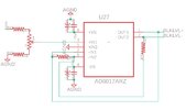
Pic of your SMD layout.....?

The outputs look pretty good and they stay within at max ±1.5mv noise levels.

150C at package surface, and a 95C/W thermal R says to me the die is hotter than the surface of the sun.
When looking at output is your scope BW restrained to 10 - 20 Mhz, and/or you are using a 1X versus a 10X
probe ? You might not see the oscillation.

NOTES 1 Stresses above those listed under Absolute Maximum Ratings may cause permanent damage to the device. This is a stress rating only; functional operation of the device at these or any other conditions above those indicated in the operational section of this specification is not implied. Exposure to absolute maximum rating conditions for extended periods may affect device reliability. 2 Specification is for device on a two-layer board with 2500 mm2 of 2 oz. copper at +25°C 8-lead SOIC package: θJA = 95.0°C/W. MAXIMUM POWER DISSIPATION The maximum power that can be safely dissipated by the AD8017 is limited by the associated rise in junction temperature. The maximum safe junction temperature for plastic encapsulated device is determined by the glass transition temperature of the plastic, approximately 150°C. Temporarily exceeding this limit may cause a shift in parametric performance due to a change in the stresses exerted on the die by the package. Exceeding a junction temperature of 175°C for an extended period can result in device failure.


Regards, Dana.
 
Last edited:
It could be that the whole ground plane around the IC is acting as a resonant circuit?

It's got long paths around components & tracks, with next to no stitching to the opposite ground - assuming that is even continuous?
 
Layout recommendations -

1655197328481.png

above from datasheet

Eval board (note 6 layer) -


Lastly you sure you have Analog Devices parts, not Chinese knockoffs. Numerous dialog
on web of various parts where high speed parts sourced out of China not up to snuff.

Possible power supply sequencing issue ?


Using low C fet probe for probing ?


Regards, Dana.
 
Last edited:
Schematic in post #1 shows no power supply? Both supply pins are capacitively coupled to ground?
I think that there is a small "+5VA" and a "-5VA" on the diagram.

It would make the diagram far easier to understand if the two op-amps were shown separately.

It's seems odd to use a really fast op-amp to buffer and invert a potentiometer. The fact that it is getting hot with no load, and the fact that 15 pF makes it hotter, makes it look like high-speed oscillation. If you get an op-amp with a much lower bandwidth, it's less likely to oscillate.

If the AD8017 does oscillate, you need a good oscilloscope to spot that it is oscillating.
 
It could be that the whole ground plane around the IC is acting as a resonant circuit?

It's got long paths around components & tracks, with next to no stitching to the opposite ground - assuming that is even continuous?
The ground is continuous on top and bottom around the component and all those small vias you see are all stitching both ground planes
Lastly you sure you have Analog Devices parts, not Chinese knockoffs. Numerous dialog
on web of various parts where high speed parts sourced out of China not up to snuff.
I am very well aware of this. I even replaced the IC with new one that I got from Digikey with same results.
It's seems odd to use a really fast op-amp to buffer and invert a potentiometer. The fact that it is getting hot with no load, and the fact that 15 pF makes it hotter, makes it look like high-speed oscillation. If you get an op-amp with a much lower bandwidth, it's less likely to oscillate.
I am leaning towards oscillation too since it gets too hot with a cap in parallel to feedback in the second stage.

What would you guys recommend for a good VF dual op-amp that is unity gain stable and low offset and temperature drift? I know there are many to choose, but looking for one that would be a good choice
 
Notice the ground is not poured everywhere in the datasheet recommendations,
rather surrounds the part ? But looking at ap note on eval board one cannot tell
if plane is void below the part or poured on the inner layers......

From datasheet -
The PCB should have a ground plane covering all unused portions of the component side of the board to provide a low impedance ground path. The ground plane should be removed from the area near the input pins to reduce stray capacitance.


Regards, Dana.
 
The ground is continuous on top and bottom around the component and all those small vias you see are all stitching both ground planes
You have a few widely scattered VIAs and many "ends" of ground plane left open. The whole thing is a resonator.

Stitching means bonding at close regular intervals!
 
For now, I replaced it with AD712 and there is no heat issue at all. Then AD712 is not a CFB type.

But would like to investigate this issue and learn why it is happening though. I have another board of the same type with same behavior
 
Status
Not open for further replies.

Latest threads

New Articles From Microcontroller Tips

Back
Top