Continue to Site

Welcome to our site!

Electro Tech is an online community (with over 170,000 members) who enjoy talking about and building electronic circuits, projects and gadgets. To participate you need to register. Registration is free. Click here to register now.

  • Welcome to our site! Electro Tech is an online community (with over 170,000 members) who enjoy talking about and building electronic circuits, projects and gadgets. To participate you need to register. Registration is free. Click here to register now.

Op-Amp circuit not working

Status
Not open for further replies.

pavjayt

Member
Hello All,

I have the attached design implemented on a PCB and it doesn't work. Could you guys let me know if I am doing it wrong?

Design is for a gain or 2.

thanks in advance.
 

Attachments

  • GainAmp.jpg
    GainAmp.jpg
    207.3 KB · Views: 230
Sure, attached is a schematic in eagle using LMH6722

Any suggestions?

All I am trying to do is to implement a gain amplifier with Gain of 2 for an input signal of 0-1V at 50MHz with out any overshoot, undershoot and ringing noise at the edges. This will be duplicated for 4 channels.

thanks
 

Attachments

  • gain2.JPG
    gain2.JPG
    110.4 KB · Views: 207
Last edited:
what is the circuit doing? Output stuck high, low, oscillating...? Circuit looks OK to me, although noise generated from R4 might cause your output to swing wildly because you are injecting it directly into the inverting node of the amplifier
 
looks like a video amp to me... the gain of 2 is needed as the 50 ohm source into the 50 ohm load cuts the signal in half. Then you double it to get it back to the original level.
 
All I am trying to do is to implement a gain amplifier with Gain of 2 for an input signal of 0-1V at 50MHz with out any overshoot, undershoot and ringing noise at the edges. This will be duplicated for 4 channels.

thanks

What is the purpose of the chain R4...R6 ?
Why two inverting opamps for a gain of 2 ? Why not using one single non-inverting circuit?
 
Gain of 2 for an input signal of 0-1V at 50MHz with out any overshoot, undershoot and ringing noise at the edges.
Challenging. Pcb layout will be critical.
 
What is the purpose of the chain R4...R6 ?
Why two inverting opamps for a gain of 2 ? Why not using one single non-inverting circuit?

The chain of R4 is used as an output signal offset adjustment. I made an exact layout on a breadboard to replicate the problem. Will post the result of it in a little while.
 
The offset trim doesn't have any effect on the output offset which is strange to me. Does anyone have a working schematic of a opamp with an adjustable gain of 2 along with adjustable offset. Basically something that replicates the circuit that I have, but tested and working?

thanks.
 
The offset trim doesn't have any effect on the output offset which is strange to me. Does anyone have a working schematic of a opamp with an adjustable gain of 2 along with adjustable offset. Basically something that replicates the circuit that I have, but tested and working?

thanks.

Try applying the offset to the + input as described here:

The method of adding a voltage to the non-inverting input can also be used to zero the offset voltage between the inputs, while injecting a current into the inverting input will not accomplish this well. The reason is that the input offset is the difference in voltage drop of two base-emitter diodes (transistors Q1 and Q2 in Figure 2 ). Because of the exponential characteristic, a large percentage change in current is needed to shift a diode-drop to the required value.

https://www.electro-tech-online.com/custompdfs/2012/12/snaa004.pdf

Thanks for that document. I followed it for non-inverting setup using an AD811 and now it works just fine except for rippling noise. The input has about 50ns and the output comes out to be 100ns settling time. Is there any way to reduce that too??

In the snapshot, CH1 is input (top) and CH3 is output (bottom)
 

Attachments

  • 2012-12-20-382.jpg
    2012-12-20-382.jpg
    1.1 MB · Views: 179
The ringing on the edges at the input is replicated (and magnified) at the output, so you would have to reduce the bandwidth of the circuit, or get ride of the ringing on the input, to reduce the ringing at the output. But, reducing the bandwidth will also reduce the rise-time of the output pulse.
 
I redesigned the circuit using AD811 and also using the tip from the TI document for offset and it works fine except for that ringing which I guess will be ok for now.

One thing I would like some suggestion on is how can I use a single power supply for different sections of my design which otherwise uses 3 different power supplies to eliminate noises between the sections. I would like to use a single +/-15V supply for both analog and digital sections of my board efficiently without propagating noise between the sections.

thanks
 

Attachments

  • Gain2.jpg
    Gain2.jpg
    189.4 KB · Views: 176
Fortunately, it is not usual to use multiple supplies for the sole purpose of addressing noise on a single circuit card assembly, unless there is a heavy load that should have its own power supply and power connections. Good layout, grounding, and bypassing techniques are the best ways to address noise in the system. The analog ground plane should be separate from the digital ground plane, joined together at only one point near to the ground pin(s) of the device(s) that use the most current and the return connection from the main power source should be located at that same point.

See also: https://www.electro-tech-online.com/custompdfs/2012/12/sloa089.pdf
 
Thanks ccurtis, I will try to follow the guidelines and use single power supply for all my sections, but with careful attention to routing and noise suppression techniques.
 
It would be great if someone can check my schematic and board layout for any modifications for improved performance and low noise.

thanks
 
Last edited:
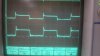
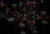
Unfortunately, I don't have the tool(s) necessary to view those files. Perhaps someone does. I want to mention, though, that the ringing in the scope image is not so much noise as it is either an impedance mismatch, or parasitic capacitances and inductances in the circuit (those that are not part of the design, but exist as by-products of lead length, PCB traces and materials, etc, used to construct the circuit) that resonate (ring) at their characteristic frequency. So, in addition to proper layout for noise, lead and trace lengths must be as short as possible, and not run too close together. Any cables into and out of the amplifier of any significant length must be constant impedance (coaxial, twin-lead, etc) cables and matched to the input/output impedance at each end.
 
Status
Not open for further replies.

Latest threads

New Articles From Microcontroller Tips

Back
Top