Continue to Site

Welcome to our site!

Electro Tech is an online community (with over 170,000 members) who enjoy talking about and building electronic circuits, projects and gadgets. To participate you need to register. Registration is free. Click here to register now.

  • Welcome to our site! Electro Tech is an online community (with over 170,000 members) who enjoy talking about and building electronic circuits, projects and gadgets. To participate you need to register. Registration is free. Click here to register now.

"Normal" uart data flow via lazer and photodiode

Status
Not open for further replies.

mik3ca

Member
I'm trying to make a circuit where my computer can send data out serially to the lazer and receive data from the phototransistor, but the bit values both ways need to be inverted (so I see it as "normal")

When the computer doesn't send data out, the lazer light must be off.
But when the UART start bit is transmitted, the lazer light goes on (this is when the computer transmits a logic low out).
I'm doing it this way so the lazer doesn't stay on forever while waiting for the computer to send data out.

Reception is similar. When the phototransistor does not detect light, then it means the computer receives a logic 1. When the phototransistor detects light, then the computer receives a logic 0.

This is my circuit so far:
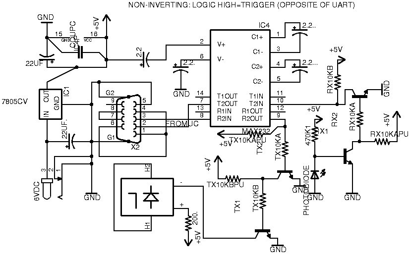
circuit.png


The question is, other than the 200 ohm resistor connected to the lazer (yes its my own symbol with an L with a picture of a diode), is there a way to calculate the optimal values of the resistors attached to the transistors? The resistor connected to the phototransistor is set to 100K, but sensitivity is not a concern because in my tests the remote light will be strong when it is aimed at the phototransistor.

So how do I calculate the optimal values of the resistors and still have bright lazer output without damaging the lazer?

The lazer is a cheap ebay 5mw lazer module from china with a resistor built onto it which I think is 80 ohms.
 
I would have considered IC's but due to the small board size I couldn't afford to fit another 14-pin IC on it.
 
I would have considered IC's but due to the small board size I couldn't afford to fit another 14-pin IC on it.
You can fit four discrete transistors and their associated base resistors AND their associated pull-up resistors, but you can't fit an single IC that would replace all those components? I don't really believe that.
 
You can fit four discrete transistors and their associated base resistors AND their associated pull-up resistors, but you can't fit an single IC that would replace all those components? I don't really believe that.

Considering I can only do single-sided PCB's nicely with limited board space and without ugly construction, yes. Have a look:

circuit.png


Yes I know there's extra ground on the top and right but I originally formatted the board size to 46x40mm but I expanded it to fit my next board size I had available to me without having to cut a new piece.

The bottom-right component is the lazer and the top right is a 7805
 
Considering I can only do single-sided PCB's nicely with limited board space and without ugly construction, yes. Have a look:

View attachment 113827

Yes I know there's extra ground on the top and right but I originally formatted the board size to 46x40mm but I expanded it to fit my next board size I had available to me without having to cut a new piece.

The bottom-right component is the lazer and the top right is a 7805
I'm not convinced because with a single-sided PCB that you etch yourself, it's even more convenient to go with an SMD IC which would free up nearly 1/4 of the lower right of your PCB. A 14-pin SOIC or TSSOP is less than 1/2 or 1/4, respectively of the size of the DIP you have on there. That's a lot of room to work with routing.

It's single sided so thru-holes arent being used to tie two layers together. Your components aren't laid out so thru-hole components jump traces nor do you ever seem to run traces between pins. You don't seem to be using any of the advantages thru-hole routing gives you. Are you afraid of SMD or something? It's not hard at all at SOIC or TSSOP sizes even if you iron tip is oversized (just means you can drag a bead of solder). All you need is a extra flux.
 
Last edited:
The thing is I sometimes have bad luck when developing my PCB to the point where traces thinner than 12mils wide vanish. I tend to widen my traces as much as possible to allow the necessary current to go through without overheating the traces. Ok, I might be a tad ridiculous with my widths but at least nothing is overheating.

I am aware of SMD but that's even worse because:

1. pins on many SMD chips are so close together and will require my board to have very small width tracks.

2. As you said, extra flux is needed just to get rid of the connections between adjacent smd pins.

3. The part needs to be held by another tool of some sorts while soldering.

You don't seem to be using any of the advantages thru-hole routing gives you

There's a big one I am using in all my designs. When I insert the components, I bend the leads so they touch the pads. Then when I solder, I don't even have to hold the component in place because the circuit board is already holding the part in for me. Also, with my designs, the odds of error are far less. Yes I get thin hairlines between PCB tracks as a result of a not-so-clean glass when doing the development but with my board, I can redefine the isolation areas by running through them with a utility knife. Ok, so by board may look messy-ish but at least after a few runs with the knife, the hairlines are gone.
 
The thing is I sometimes have bad luck when developing my PCB to the point where traces thinner than 12mils wide vanish. I tend to widen my traces as much as possible to allow the necessary current to go through without overheating the traces. Ok, I might be a tad ridiculous with my widths but at least nothing is overheating.

I am aware of SMD but that's even worse because:

1. pins on many SMD chips are so close together and will require my board to have very small width tracks.

2. As you said, extra flux is needed just to get rid of the connections between adjacent smd pins.

3. The part needs to be held by another tool of some sorts while soldering.


There's a big one I am using in all my designs. When I insert the components, I bend the leads so they touch the pads. Then when I solder, I don't even have to hold the component in place because the circuit board is already holding the part in for me. Also, with my designs, the odds of error are far less. Yes I get thin hairlines between PCB tracks as a result of a not-so-clean glass when doing the development but with my board, I can redefine the isolation areas by running through them with a utility knife. Ok, so by board may look messy-ish but at least after a few runs with the knife, the hairlines are gone.

Well if your etching process is limiting your trace widths, there's not much way around that. To answer your original question, your laser power isn't affected by the transistors used to invert logic since the only one immediatley influencing the laser is the 200 ohm resistor and the closest transistor. Obviously you should be sizing the 200ohm resistor according to your laser diode's voltage drop and current limits.

Just make sure that one transistor closet to the laser fully conducts which shouldn't be too difficult. The main thing with all your other (inverting) transistors is just to make sure your pull-ups aren't so big that the transitions are too slow for your UART signal. I don't think you need to need to go below 3kohm or 4.7kohm to maintain the speed (depends on your baud rate though). Go higher values to limit power dissipation but I wouldn't go higher than 10kohms. There's a lot of gut-feel to it since there's no real right, best answer.
 
Is my hardware setup OK for 9600 baud or do I need to lower the resistor connected to the phototransistor?
No way to tell without info about both your phototransistor and your laser diode. Why don't you just try it?
 
I did at various different baud rates and I'm getting incorrect data
It goes without saying to first test it first with regular, manually toggled logic HI and LO state before using serial messages just to make sure that something, anything can get through.

Did you look at the output signal of the receiver on an oscilloscope and compare it to the input signal?

Also scope the raw output of the phototransistor. It's possible for your laser module to not be able to turn on and off fast enough and if your photo transistor is suitable for the task then it's output will show you what the laser diode is doing (of course, if your phototransistor is not suitable you'll also get garbage).

This should also let you know if your ambient lighting is messing things up. Either because of flickeriing indoor lights disrupting the transmission or ambient light simply causing the phototransistor to always be on. Test in the dark.
 
Last edited:
sadly I have no oscilloscope. How fast are typical lazer modules? I bought mine on ebay and they came with no manual or a number for me to look up.
 
sadly I have no oscilloscope. How fast are typical lazer modules? I bought mine on ebay and they came with no manual or a number for me to look up.
I don't know but a cheap visible laser module (hell, any probably most visible laser modules) are not optimized for speed because we don't use visible light for communications. It might not even be a measured parameter for such things. Infrared is more popular for communications due to the availability of detectors, and fiber optic materials.

How far are these things anyways? Because you can get infrared LEDs (not laser diodes) and matching photodiodes cheaply that you do know the speed and other specs for. They are available in very narrow transmission angles (+/-3 degrees) as well as reception angles (+/- 10 degrees). The photodiodes also come in infrared transparent but ambient opaque packaging so the ambient light doesn't mess them up. Combined with the narrow reception angle, you can also use your aim to ignore random infrared sources.

This photodiode is the same one used in the Reference Photodiode Amplifier design I linked to in your photodiode amplifier post. That simple design gets 1Mhz bandiwdth which is good enough to transmit the first 50 harmonics of the 9600bps square wave.
 

Attachments

  • OSRAM SFH 213 FA.pdf
    268 KB · Views: 88
  • OSRAM SFH 4350.pdf
    382.6 KB · Views: 77
  • OSRAM SFH 4550.pdf
    385.2 KB · Views: 73
Last edited:
The transmission will be up to about 200 meters but at least 5 meters. but on average, about 20 to 100 meters.
 
The transmission will be up to about 200 meters but at least 5 meters. but on average, about 20 to 100 meters.
Hmm, yeah need lasers for that. You might want to build a linear photodiode amp that you know works and use it to evaluate how fast that laser diode is actually turning on and off. Unfortunately, to do that you need to be able to read the output of the photodiode amp which means you need an oscilloscope.

As it is, without access to an oscillscope you have no way to know if the problem is sensitivity, beam strength, ambient lighting issues, or rise/fall times issues.
 
Status
Not open for further replies.

Latest threads

New Articles From Microcontroller Tips

Back
Top