Continue to Site

Welcome to our site!

Electro Tech is an online community (with over 170,000 members) who enjoy talking about and building electronic circuits, projects and gadgets. To participate you need to register. Registration is free. Click here to register now.

  • Welcome to our site! Electro Tech is an online community (with over 170,000 members) who enjoy talking about and building electronic circuits, projects and gadgets. To participate you need to register. Registration is free. Click here to register now.

Non-overlapping Two-Phase Clock Generator Layout

TW1

New Member
Can someone help me, if this CMOS circuit (attached) implementation is correct? for a Non-overlapping Two-Phase Clock Generator
Below is the schematic diagram of the CMOS logic ckt.
1690521509121.png
 

Attachments

  • CMOS Circuit.jpg
    CMOS Circuit.jpg
    167 KB · Views: 135
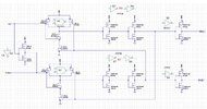
Inverters are normally buffered, so there are in effect three stages. What you have shown in the circuit diagram with MOSFETs would be unbuffered inverters.
https://www.ti.com/lit/ds/symlink/sn74hc04.pdf
https://www.ti.com/lit/ds/symlink/sn74hcu04.pdf

If you compare those, the diagrams shows one as being bufferend and on not.

The unbuffered one is marginally faster, but that is with quite a big capacitive load of 50 pF. With a smaller load, the unbuffered one would be distinctly faster than the buffered one.

The circuit that you have shown relies on the propagation delay to give the timing gap between the phases. The gap* will be around three gate delays, or 30 ns. I don't know if that is enough for your application, as there is usually a reason for a non-overlapping clock, which might need more time.

As the gate delay depends on temperature and supply voltage, you will find the phase gap varying and it could become insufficient.

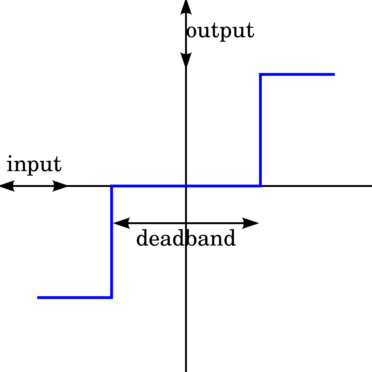
As an example of non-overlapping clocks, something like this
/https://www.onsemi.com/pdf/datasheet/ncv7547-d.pdf
has preset times from one MOSFET turning off to another turning on, called the blanking times, of 1, 2, 3 or 4 μs. That is the time allowed so that you don't get both MOSFETs conducting at the same time, which would short the supply. The smallest time programmed into that IC is 30 times longer than your circuit will give.

*I'm not sure of the correct term for the opposite of overlap.
 
  • Like
Reactions: TW1
This is my logic ckt and the waveform I'm getting
Looks like there's a small amount of non-overlap, but you'd have to zoom in on the transition points to see how much.
What non-overlay time are you looking for?
 
  • Like
Reactions: TW1
If you want a big fat deadband without lotsa gates, a small R-C network will get you microseconds (or tens of nanoseconds) of delay repeatably and cheap. Are you looking for a discrete component circuit or for something within a CPLD or FPGA?

AND - five posts in - what is the clock frequency, and the minimum and maximum deadband times you can work with?

ak
 
  • Like
Reactions: TW1
If you are working with modern processrs most have configurable PWMs with dead band
control :

1690585893730.png

ph1 and ph2 have non overlapping, set to 8 clocks of dead band.


Regards, Dana.
 
  • Like
Reactions: TW1
Thanks for all your input, I truly appreciate it. This is just one of our lab experiments, and we needed to do pre-simulation (schematic layout) and post-simulation (cell layout). I'm just seeking some help from the experts to determine if the implemented CMOS circuit provided is correct based on the schematic of the logic circuit.
1690600850091.png

1690600954540.png
 

Latest threads

New Articles From Microcontroller Tips

Back
Top