blue6x
New Member
As we all know, on transistors, the current flows from the collector and the base down to the emitter and then around the whole circuit back again to that base and collector.
Also, That the base emitter junction, can be assumed as 07 V for silicon while the base collector junction is normally open...
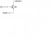
Now, what if the transistor configuration happens to be on that attached file, whereas the input is fed to the emitter, and the output is connected at the collecter. There is no other way to move the current but to pass it in the reverse operation in contrast to the known principle.
How could this be possible, and what are the possible output.
Also, That the base emitter junction, can be assumed as 07 V for silicon while the base collector junction is normally open...
Now, what if the transistor configuration happens to be on that attached file, whereas the input is fed to the emitter, and the output is connected at the collecter. There is no other way to move the current but to pass it in the reverse operation in contrast to the known principle.
How could this be possible, and what are the possible output.